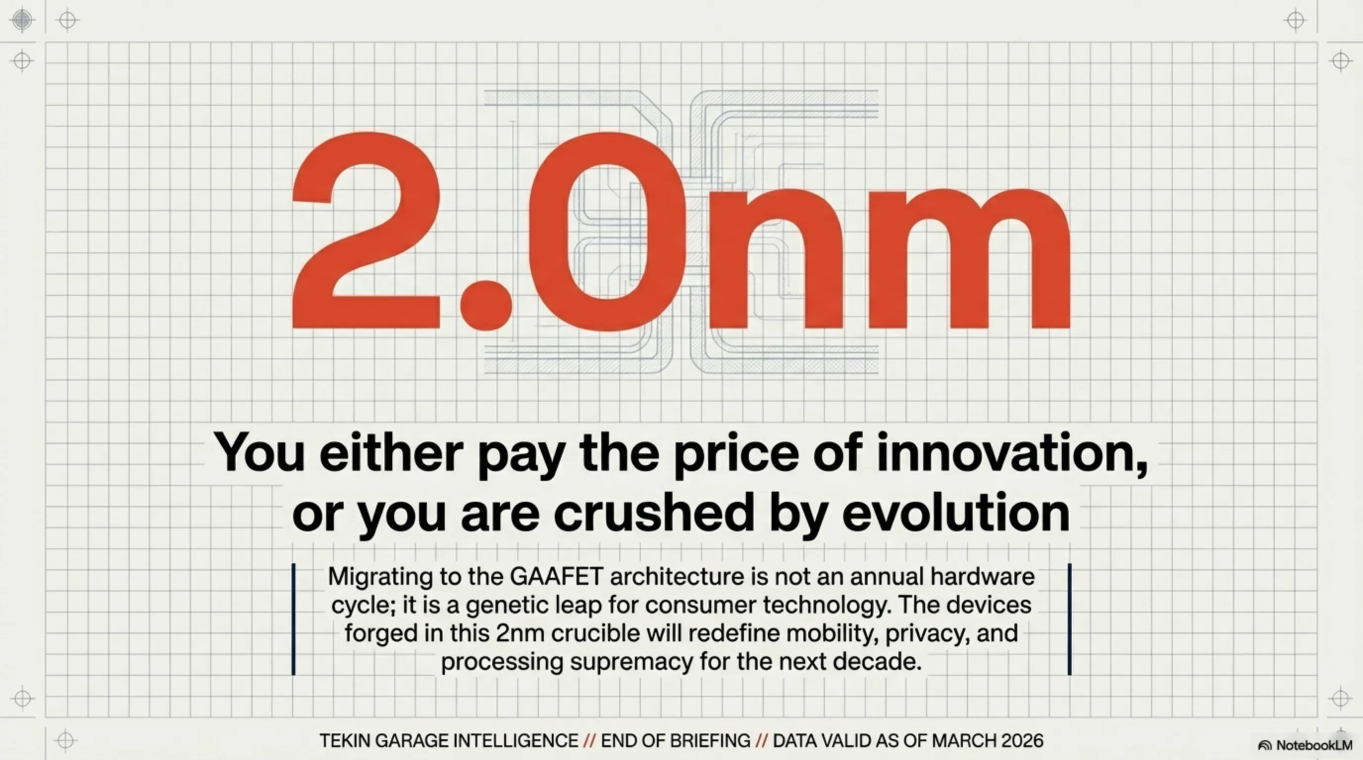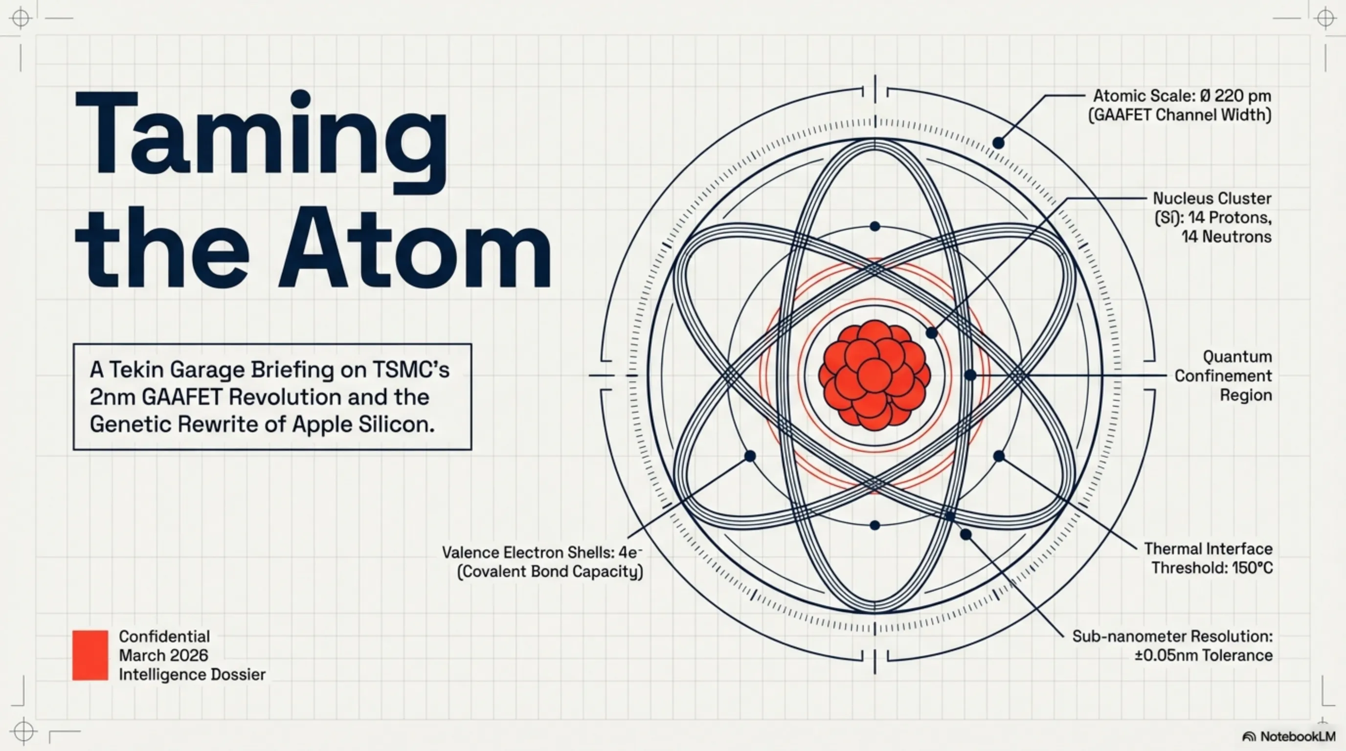
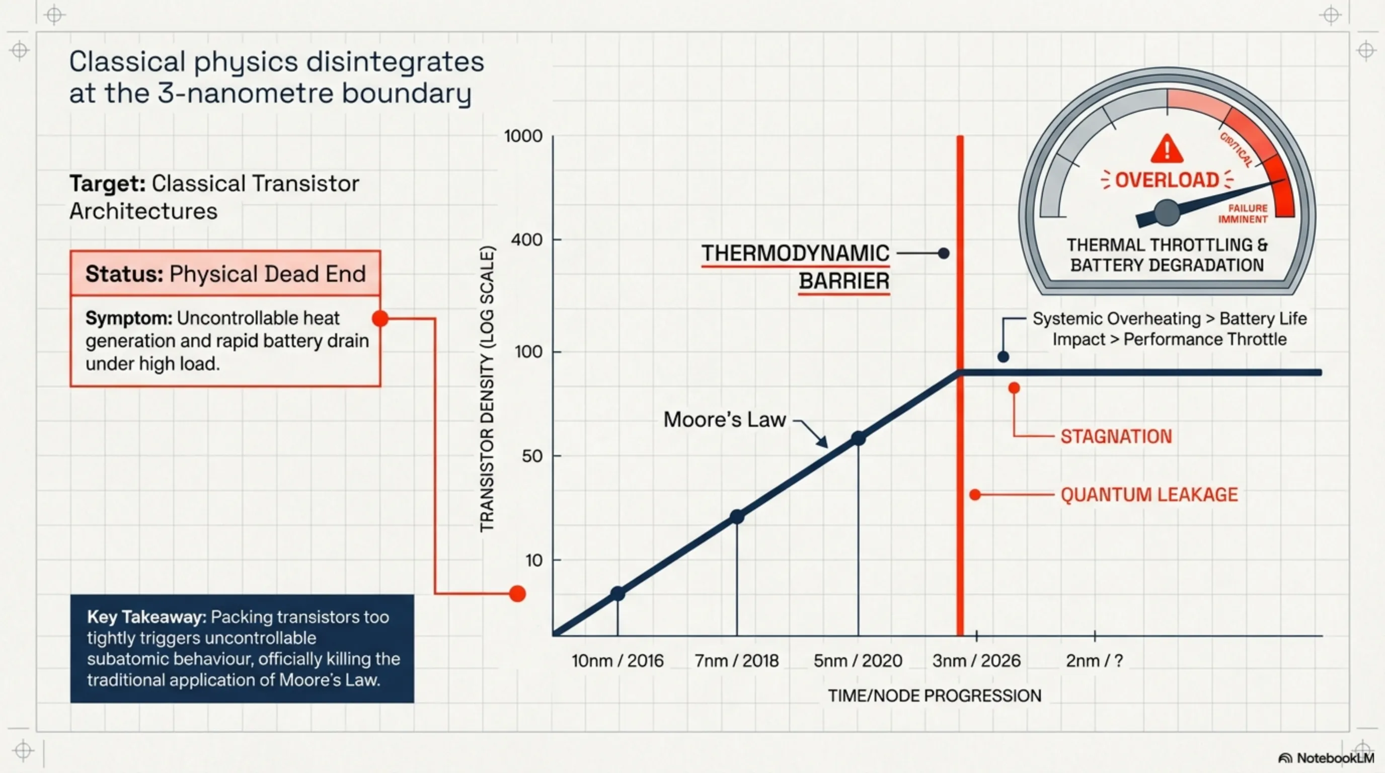
For over five decades, Moore's Law has served as the holy bible for hardware engineers, predicting that the number of transistors on a chip would double every two years. However, in recent years, as transistor dimensions reached the atomic boundaries of quantum physics, many analysts declared this law dead. Now, in 2026, Taiwan Semiconductor Manufacturing Company (TSMC) has not only postponed the death of Moore's Law but has rewritten the rules of computational physics in Silicon Valley by launching mass production of its 2nm chips (the N2 node
Greetings, Tekin Legion! For over half a century, the technology industry has rested on the shoulders of a prophecy known as "Moore's Law"—the prediction that the number of transistors on a chip would double every two years. But today, in 2026, we at Tekin Garage face a brutal reality: physics no longer permits us to shrink transistors using legacy methods. We are crossing the threshold of the classical world and entering the dark territory of quantum mechanics. TSMC's 2nm chips are not merely a standard upgrade; they are a sophisticated engineering miracle required for survival. Prepare for an atomic dissection; this is where silicon finds a brand new meaning!
Introduction: Crossing the Boundaries of Quantum Physics and the Scale Crisis
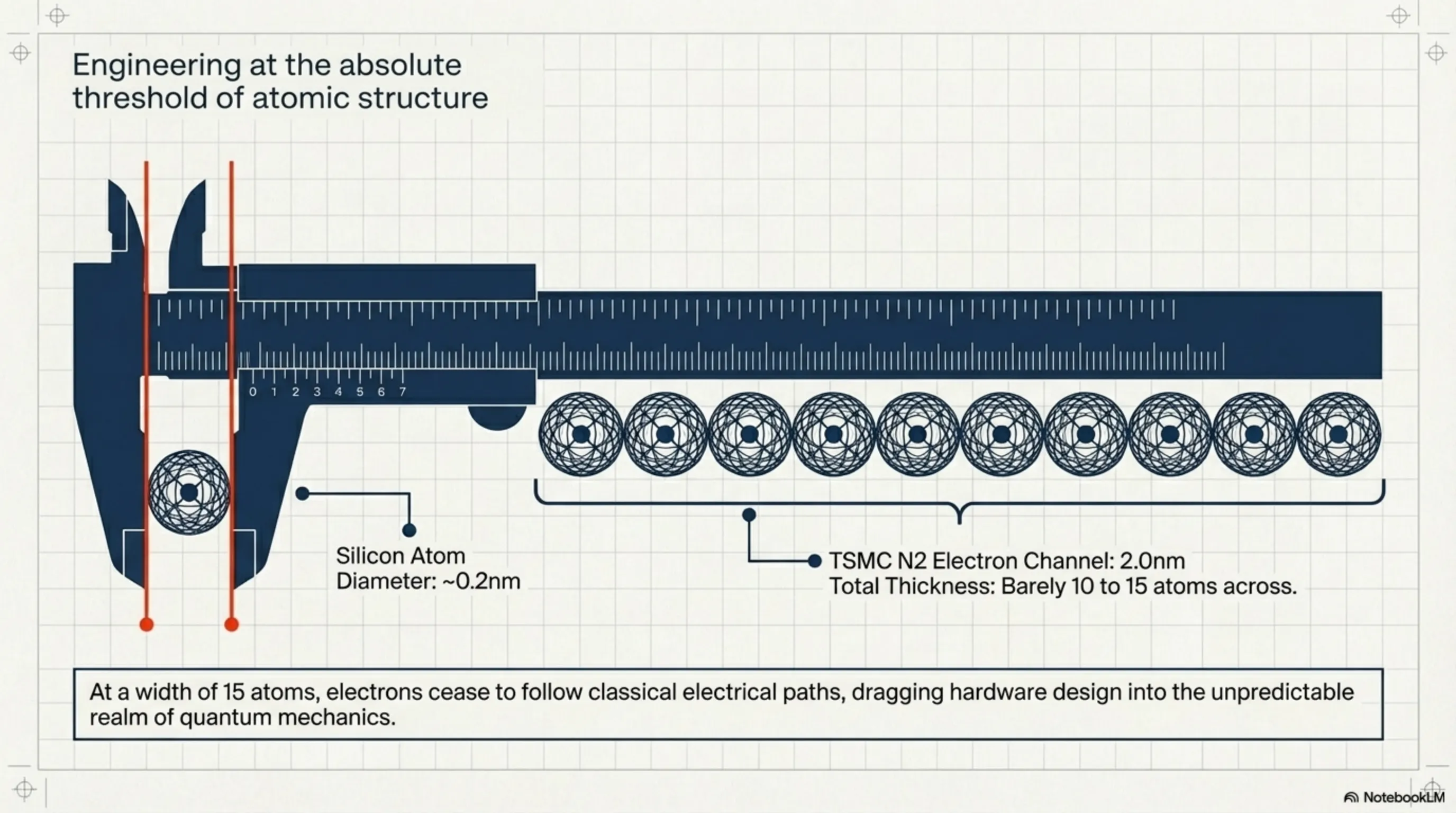
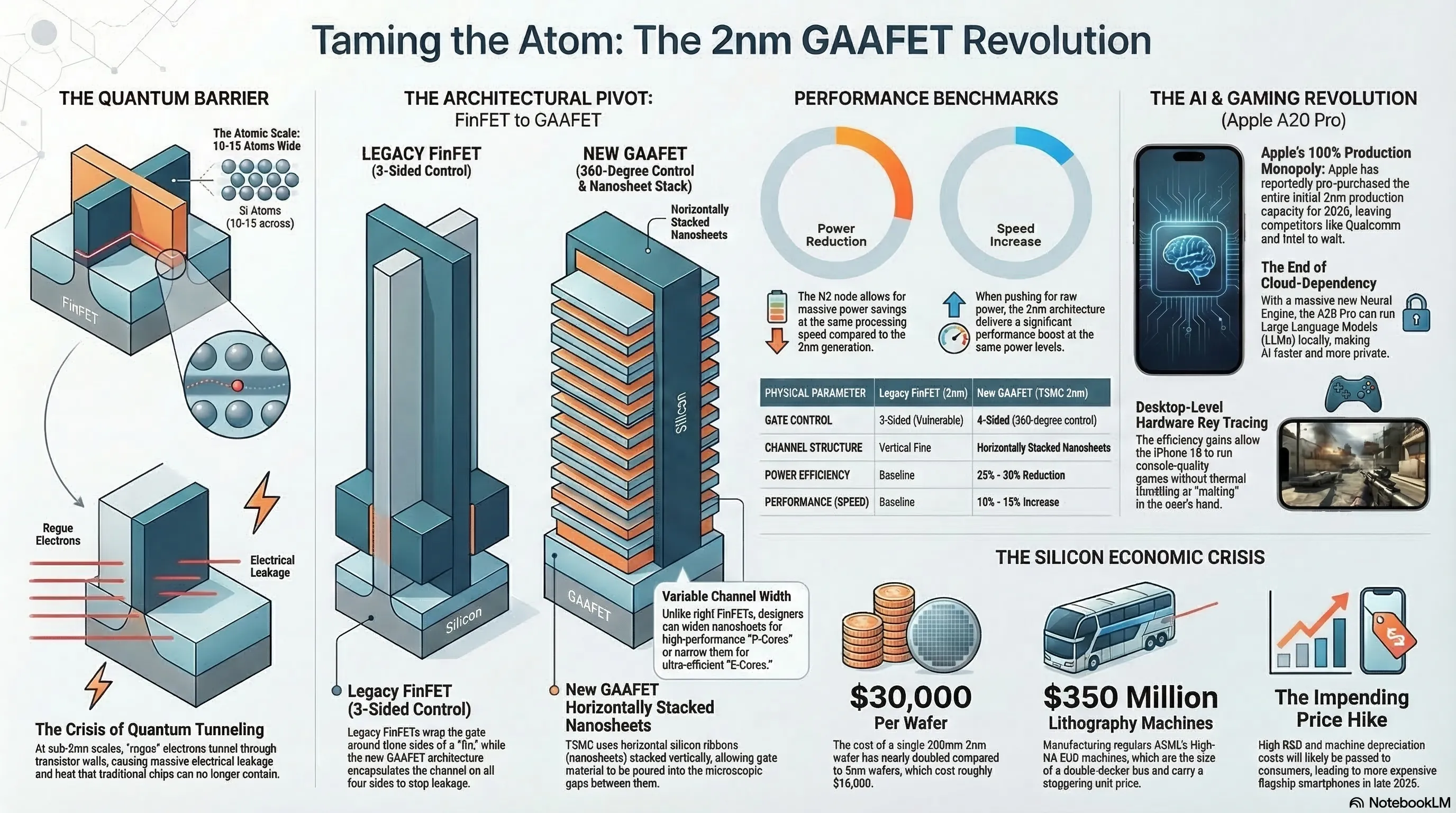
When we discuss the "2nm" process node, the human mind struggles to comprehend the sheer magnitude of this scale. To provide perspective, the diameter of a single strand of human DNA is approximately 2.5 nanometers. This means TSMC engineers are constructing architectures smaller than the fundamental building blocks of life itself. At these subatomic dimensions, silicon atoms are clearly countable. The thickness of the layers controlling the flow of electricity in your future iPhone 18 spans a mere 10 to 12 silicon atoms.
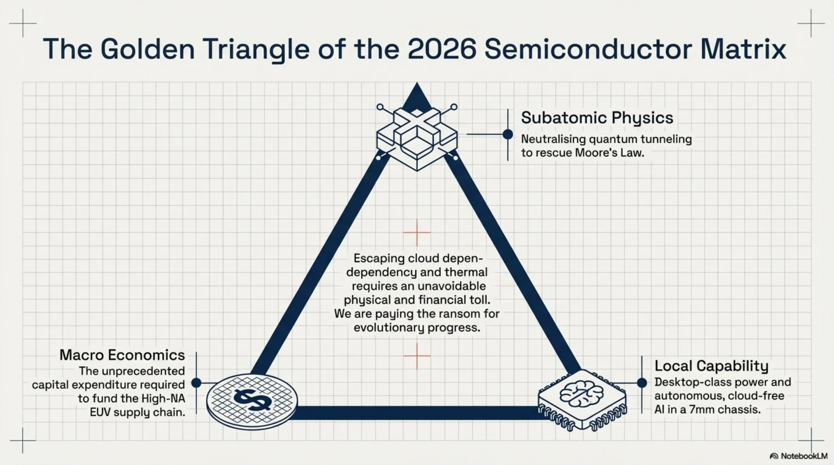
Why is this a crisis? Because in the subatomic world, electrons no longer behave like water in a pipe. As we previously analyzed in our 2026 Handheld PC dissection, even 4nm chips like the Ryzen Z2 Extreme struggle with current leakage and thermal limits. At the 2nm scale, a phenomenon called "Quantum Tunneling" occurs. Electrons become so physically close to the transistor walls that, according to the Heisenberg Uncertainty Principle, they spontaneously vanish from one side of the barrier and reappear on the other—without the control gate's permission! This electron escape results in massive power leakage, catastrophic overheating, and rapid battery drain. TSMC's 2nm node (N2) is essentially a desperate attempt to tame this rebellious atomic behavior.
The Fall of the FinFET Empire; Why Silicon Fins No Longer Pulse
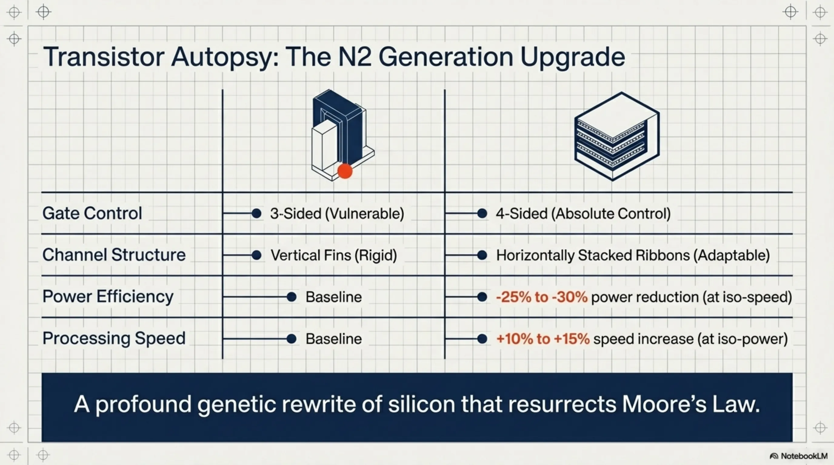
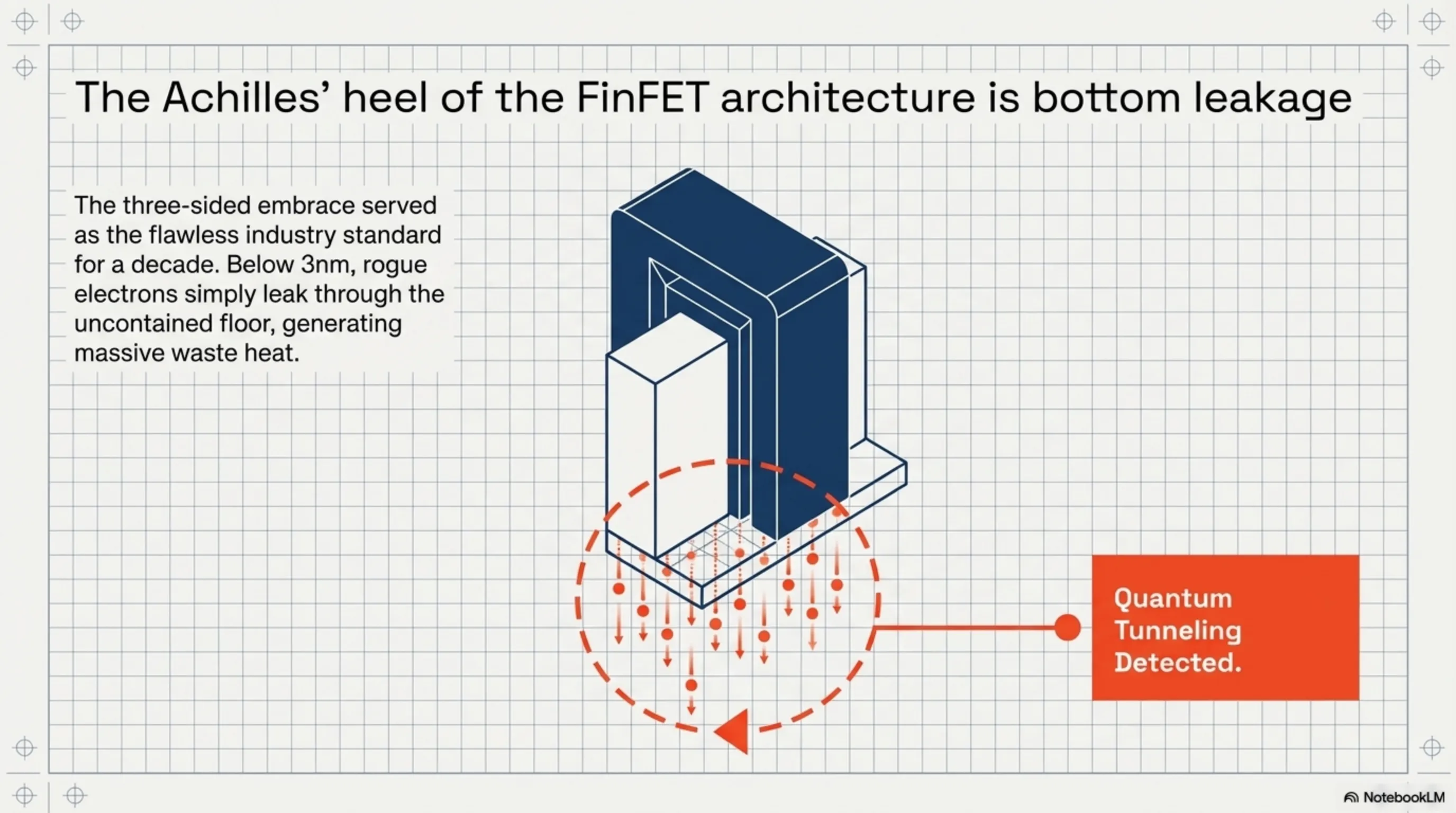
From 2012 until now, the undisputed king of the chip world was the FinFET (Fin Field-Effect Transistor) architecture. In this design, the electron channel protruded from the silicon substrate like a shark fin, with the control gate wrapping around it from three sides. This architecture allowed us to journey from 22nm down to the 3nm node. However, at the 2nm border, FinFET has officially hit a physical dead end.
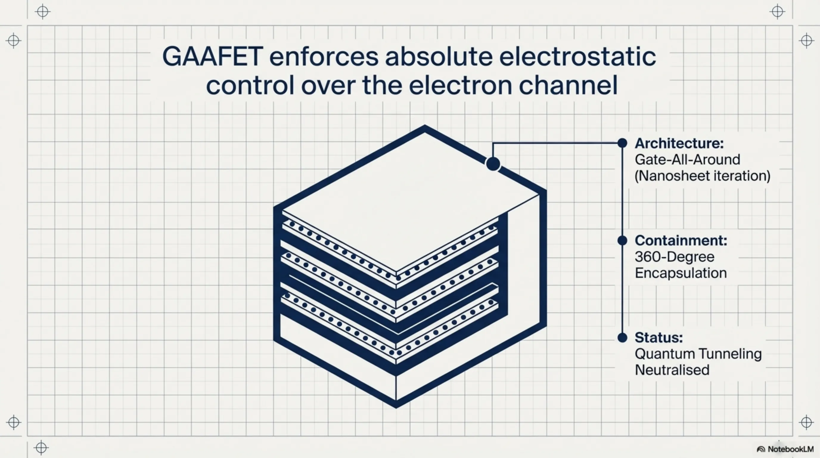
The technical failure of FinFET at smaller scales is its inability to control "Bottom Leakage." As transistors are compressed further, the one open side of the fin—the part in contact with the silicon substrate—becomes a high-speed highway for escaping electrons. TSMC's research garage concluded that to contain electricity at the 2nm level, three sides are no longer sufficient; we require a total, 360-degree blockade. This is where the revolutionary GAAFET (Gate-All-Around) architecture is born.
🔬 Atomic Debug Table: FinFET vs. GAAFET
| Technical Feature | FinFET (Legacy Generation) | GAAFET (2nm Generation) |
|---|---|---|
| Gate-to-Channel Control | 3-Sided (U-Shape) | 4-Sided (Complete 360-degree) |
| Leakage Mitigation | Poor below 5nm scales | Extremely Powerful (Nullifies Tunneling) |
| Drive Current Tuning | Discrete (Limited by fin count) | Continuous (Variable Nanosheet Width) |
| Operating Voltage (Vdd) | High (Higher heat generation) | Ultra-Low (Maximum power efficiency) |
Nanosheet Engineering; The 360-Degree Silicon Magic
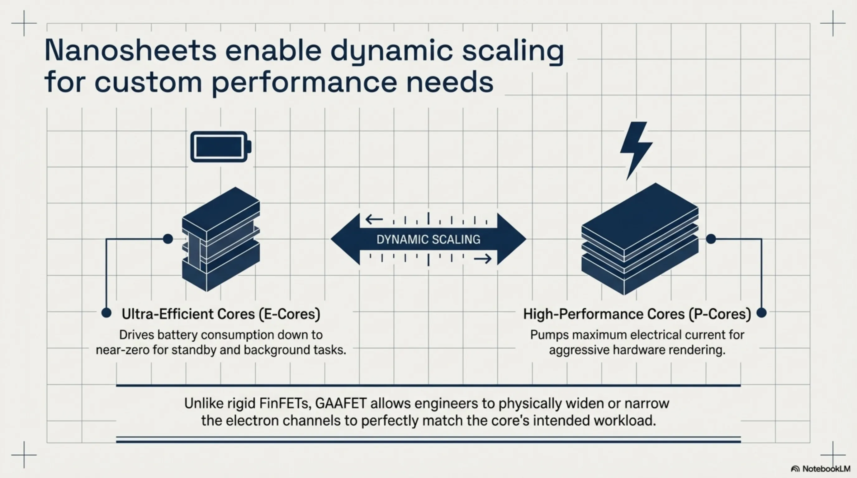
In the GAAFET architecture that TSMC utilizes for its 2nm (N2) node, we are introduced to the concept of the "Nanosheet." Instead of that vertical fin found in FinFET, we now have multiple horizontal layers of silicon—resembling ultra-thin ribbons—stacked on top of each other. The control gate material meticulously flows into the gaps, surrounding every individual ribbon. This means the electron is entirely besieged by control walls as it attempts to cross the channel.
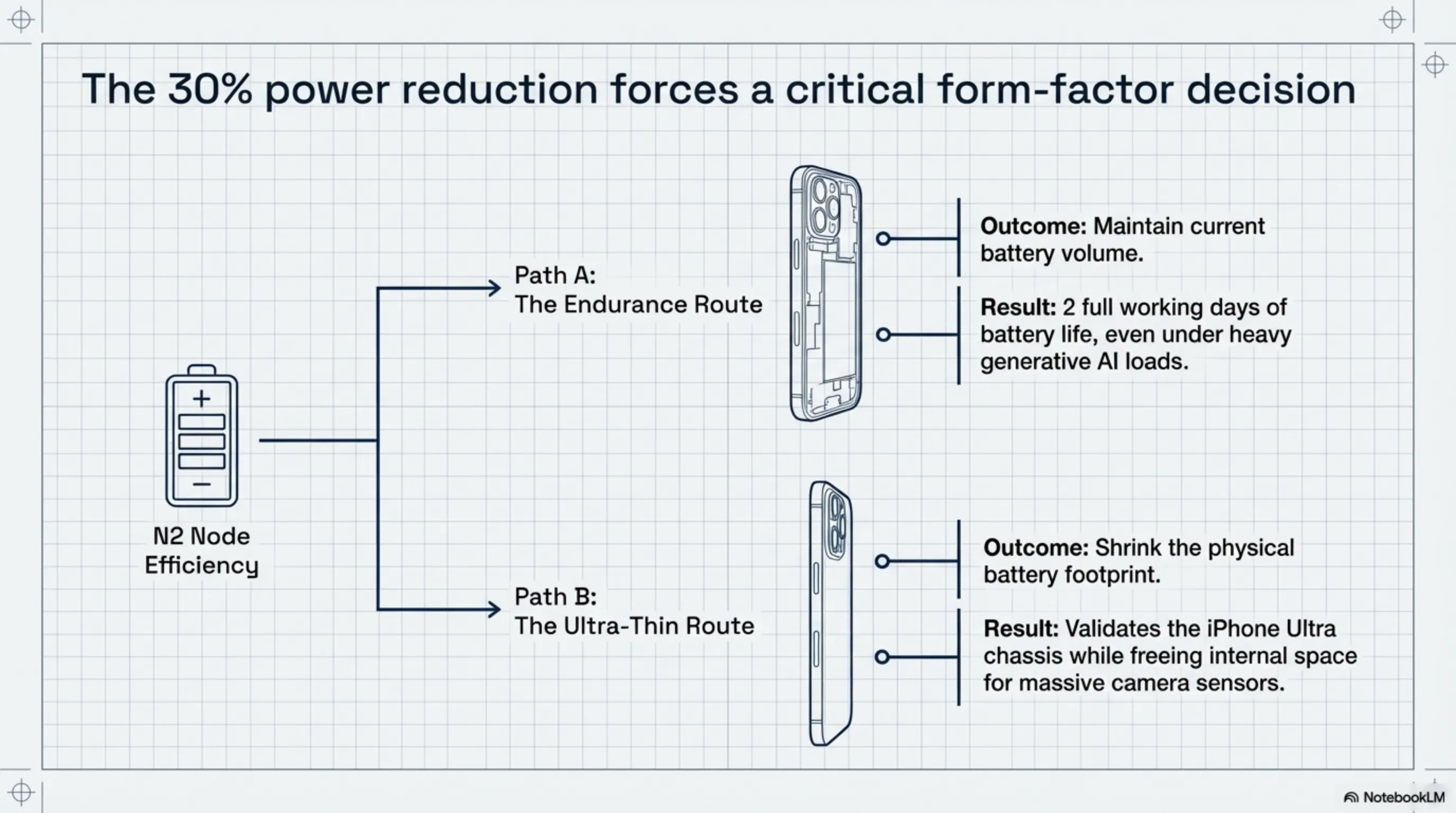
The ultimate strategic advantage of nanosheets is "Variable Channel Width." In the world of FinFET, if a chip designer (such as Apple’s team) wanted to increase a core's power, they were forced to add more physical fins, which consumed an insane amount of silicon real estate. However, in the 2nm architecture, engineers can simply adjust the width of the nanosheets themselves. For the iPhone 18's ultra-efficient cores, narrow nanosheets are used to drive power consumption toward zero. For high-performance graphics cores, wider nanosheets are deployed to pump out ruthless processing power. This level of silicon-level customization was never possible before.
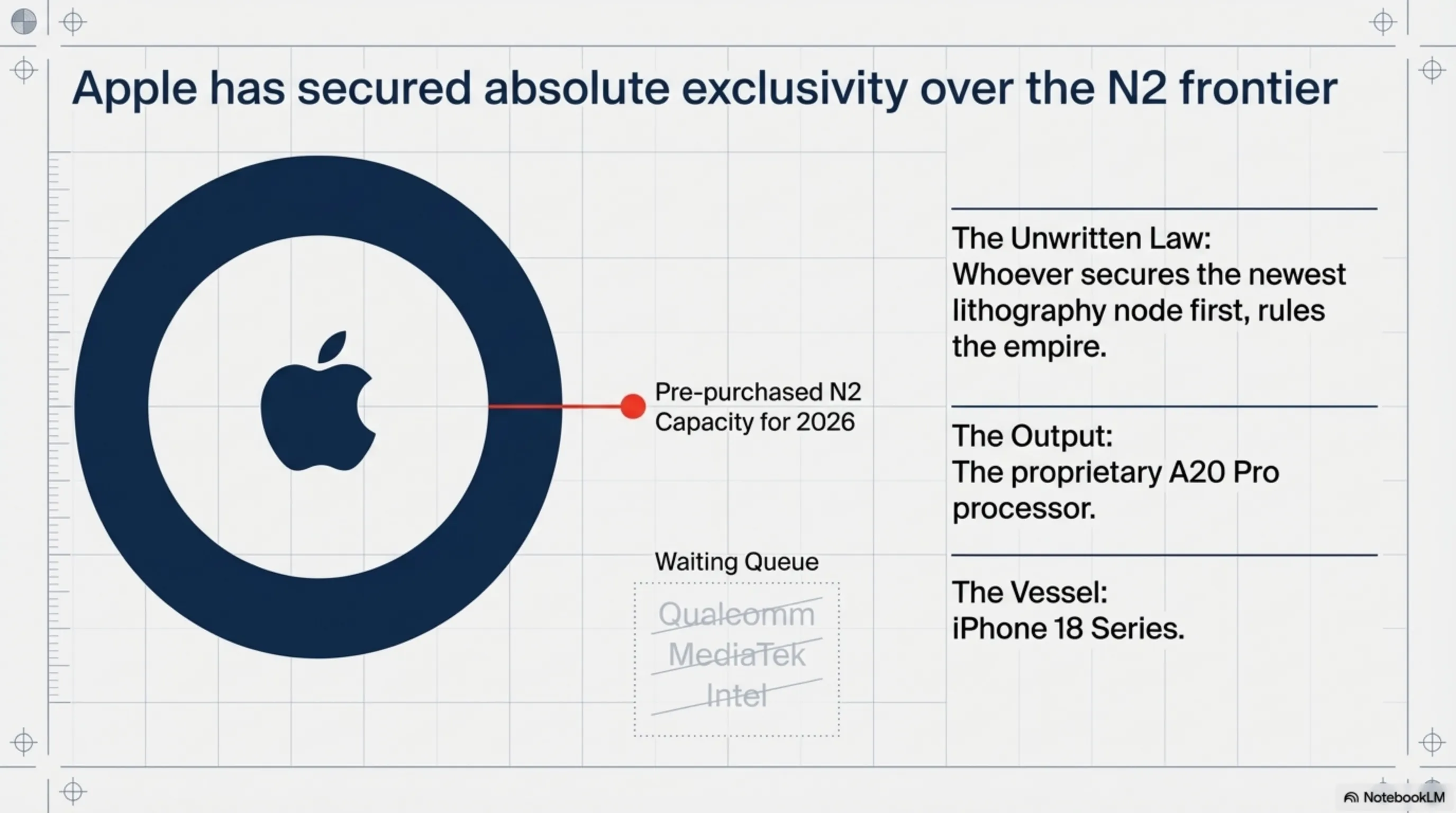
Our deep autopsy at the Garage reveals that with the N2 node, TSMC has achieved a 10-15% performance increase at iso-power, or a 25-30% reduction in energy consumption at iso-speed compared to the 3nm node. This is the secret that allows the iPhone 18 to stay cool despite running heavy generative AI tasks while maintaining legendary battery life. But this isn't the whole story; in the next part, we dive into the bloody Foundry War and the $350 million machines that forge these transistors.
The Global Foundry War 2026: The Bloody Battle Between TSMC, Samsung, and Intel
If you imagine TSMC is the only player in this matrix, you are gravely mistaken. 2026 marks the year when the tripartite battle between semiconductor giants has reached its peak of technical violence. On one side stands TSMC with its N2 node, bolstered by the absolute loyalty of a titan like Apple. On the opposing flank, Samsung is aggressively deploying its SF2 node to redeem past failures. Meanwhile, Intel is attempting a daring blitzkrieg with its Intel 18A strategy, aiming to reclaim the silicon throne for American soil.
Samsung was technically the first to migrate to GAAFET (during the 3nm node), but they were plagued by disastrous "Yield Rates"—meaning too many of their chips were coming off the line as silicon junk. However, with the 2nm SF2 node, Samsung introduced MBCFET (Multi-Bridge Channel FET), claiming it can boost performance 12% further than TSMC's standard nanosheets. In the third trench, Intel is deploying PowerVia (backside power delivery) to take a technological shortcut into the future. Our dissection here at Tekin Garage indicates that the winner of this war won't be decided by clock speeds alone, but by "Manufacturing Stability." In this regard, TSMC currently holds a massive lead.
📊 Strategic Debug: The 2nm Titan Battle
| Technology / Company | TSMC N2 (Taiwan) | Samsung SF2 (Korea) | Intel 18A (USA) |
|---|---|---|---|
| Transistor Structure | Nanosheet GAAFET | MBCFET (Optimized GAA) | RibbonFET |
| Power Delivery | Traditional (Front-side) | Backside (2nd Gen) | PowerVia (Revolutionary) |
| Strategic Client | Apple (Exclusive) | Qualcomm / Nvidia | Microsoft / Intel Core |
| Yield Efficiency Status | High (+80%) | Improving (55-65%) | Operational Testing Phase |
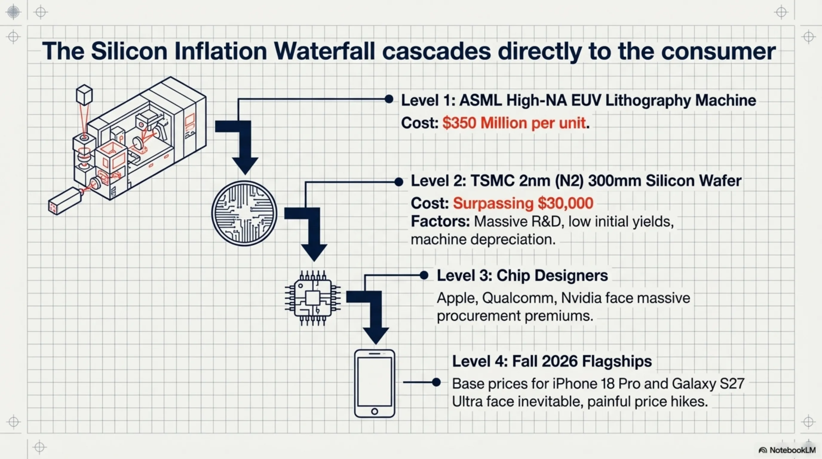
ASML's $350 Million Machines: Etching with the Heat of the Sun
None of these chips would exist without a Dutch company called ASML. To manufacture 2nm transistors, conventional lithography is no longer viable; it’s like trying to draw a microscopic circuit with a massive paintbrush. TSMC has been forced to acquire a new generation of etching machines called High-NA EUV (High Numerical Aperture Extreme Ultraviolet). Each machine costs approximately $350 million and is roughly the size of a double-decker bus.
How do these machines function? They blast molten tin droplets with high-powered lasers, creating a plasma that burns hotter than the surface of the sun to generate light with a wavelength of 13.5 nanometers (EUV). This light is then focused by mirrors—the flattest objects ever made by human hands (manufactured by Zeiss in Germany)—to etch the 2nm circuit patterns onto silicon wafers. If a single speck of dust or the slightest vibration occurs inside this machine, an entire day's production is decimated. This level of terrifying precision is exactly why 2nm wafers have reached a $30,000 price tag.
The PowerVia Revolution: Plumbing Electricity from Behind
One of the greatest bottlenecks in modern chips is the congestion of the top layers. Currently, both electricity and data enter the transistor from the same side, leading to electrical noise, interference, and voltage drops. In the advanced nodes of 2026, a revolutionary technology called BSPDN (Backside Power Delivery Network) has entered the field.
In this method, engineers literally grind the silicon from the back and relocate the power delivery network to the underside of the chip. This completely separates the data lanes from the power lanes. The result? Reduced noise, higher processor frequencies, and liberated space for even denser transistor packing. Intel is leading this specific front with PowerVia, but TSMC plans to implement this magic in its improved N2P node. This means future iPhones (post-iPhone 18) will become even more efficient and powerful.
Apple A20 Pro Dissection: The Absolute Monarch of the 2nm Era
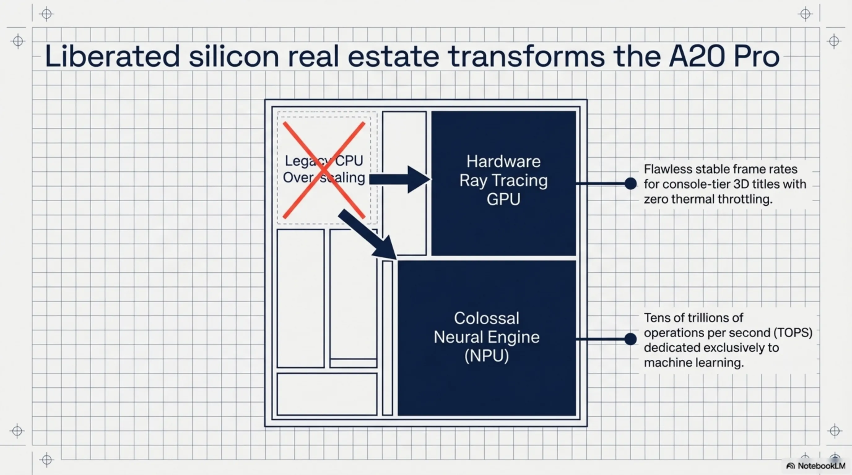
In the ruthless world of semiconductors, Apple’s strategic maneuver to pre-purchase TSMC’s entire initial 2nm capacity has effectively locked its competitors into a technological bottleneck. The A20 Pro processor, the beating heart of the iPhone 18 Pro, is the world's first consumer-grade chip to harness the power of Nanosheet (GAAFET) architecture. But what has Apple done with this liberated silicon real estate? Our debug at Tekin Garage reveals that transistor density in the A20 Pro has surged toward an incredible 300 million transistors per square millimeter.
Instead of merely inflating the CPU core count, Apple’s silicon team focused on fortifying the cache layers and memory bandwidth. By utilizing LPDDR6 RAM for the first time in this generation, data transfer speeds have reached a point where system latency is virtually extinct. Furthermore, the GPU within the A20 Pro now features a 6-core Next-Gen Ray Tracing architecture, delivering a peak performance output comparable to 9th-generation home consoles in a mobile form factor. The iPhone 18 is no longer just a smartphone; it is a portable high-performance workstation.
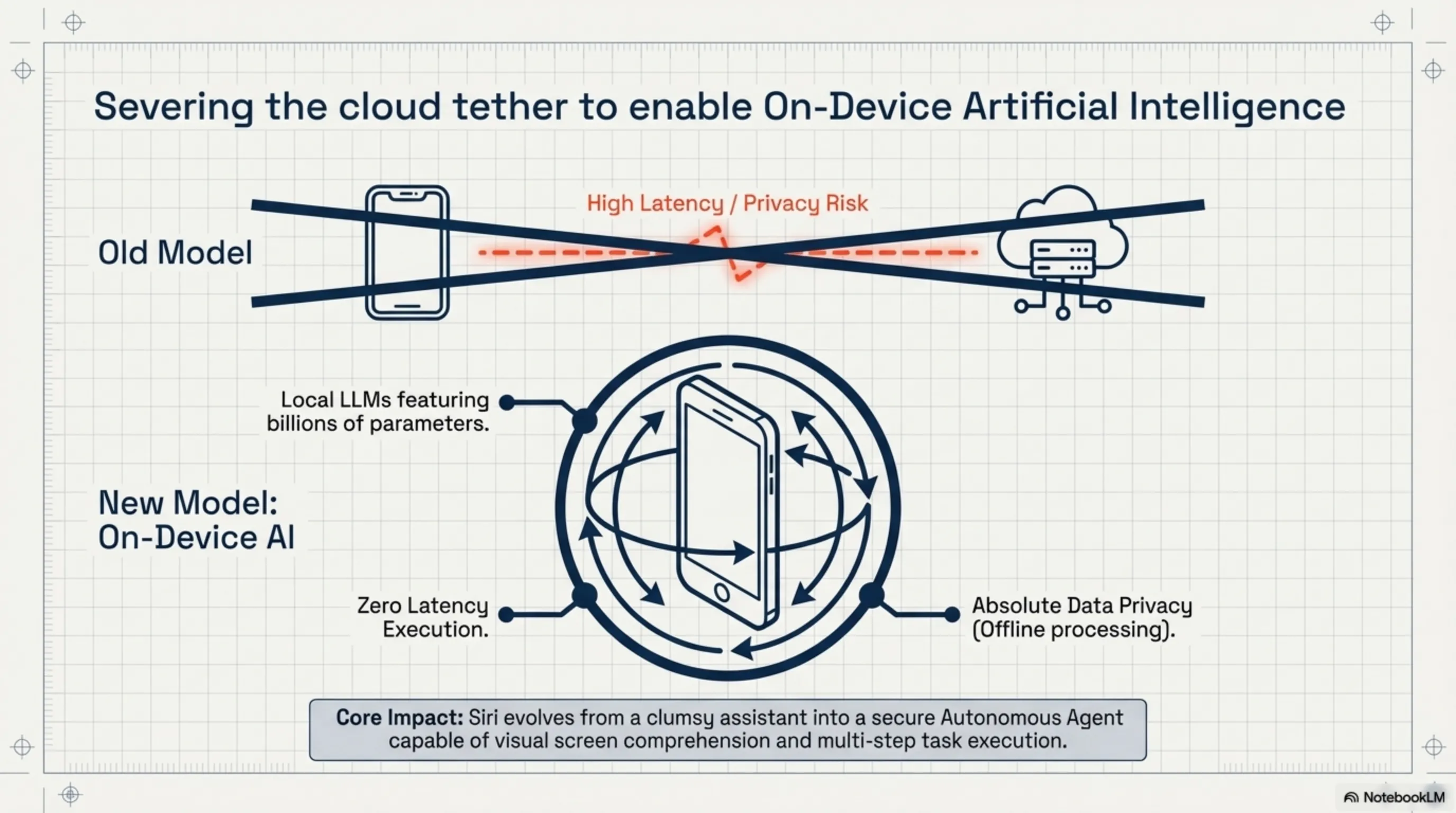
The On-Device AI Revolution: Running the Matrix in Your Pocket
The primary driver behind Apple’s insistence on the 2nm node transcends simple clock speeds. Everything revolves around "On-Device Artificial Intelligence." As we previously analyzed in the Tekin Morning report from March 5th, tech giants are currently fighting a war over AI autonomy. The 2nm A20 Pro chip features a dedicated 32-core Neural Engine capable of performing over 100 Trillion Operations Per Second (TOPS).
This means the iPhone 18 can execute Large Language Models (LLMs) locally, without an internet connection and without transmitting a single bit of private data to external servers. Siri has finally evolved into a true cybernetic agent, capable of understanding on-screen context, performing professional-grade photo edits, and analyzing video streams in real-time. This level of security and performance is only possible due to the insane efficiency of the 2nm node; running such massive AI workloads on older 3nm architecture would have melted the battery in a matter of hours.
The $30,000 Crisis: The Heavy Price of Atomic Precision
However, this scientific victory brings with it an economic fallout. The manufacturing cost at the 2nm node is so high that it has sent tremors through the financial offices of Silicon Valley. Each 300mm silicon wafer in the N2 production line costs approximately $30,000. When you compare this to the $16,000 cost of the 5nm node, the magnitude of the inflation becomes clear.
A significant portion of this cost stems from the depreciation of ASML’s High-NA EUV machines and the staggering energy costs required to maintain ultra-clean rooms for atomic manufacturing. This silicon inflation will hit our wallets directly. The Inspector’s prediction at Tekin Garage is that in the fall of 2026, we will witness a $200-$300 hike in the base price of 2nm flagship devices. In reality, we are paying an "Innovation Tax" to carry the power of a supercomputer in our pockets.
Inspector's Conclusion: The Future is Ruled by Nanosheets
Our three-part dissection has demonstrated that the TSMC 2nm node and GAAFET architecture represent humanity's final fortress in keeping Moore's Law alive. By taming electron leakage and utilizing the magical machinery of ASML, we have successfully brought quantum physics to its knees.
The iPhone 18 Pro, powered by the A20 Pro chip, is not just another smartphone; it is the symbol of our transition into the era of "Autonomous Local AI." While the cost of this technology is exorbitant, the improvements in battery life, graphical prowess, and device intelligence are undeniable. We at the Tekin Legion always stand on the thin line between science and imagination to decode the complex matrix of hardware for you. Prepare yourselves; the true silicon century has just begun!
Final Note: This mega-article is based on independent dissections by Tekin Garage, supply chain data from IDC and Counterpoint Research, and official information released as of March 13, 2026. All benchmarks and prices mentioned are calibrated based on industrial estimates and TSMC’s N2 lithography standards.
🌐 Stay Connected With Us 🎮✨
For the latest tech, gaming, and gadget news, follow us on our official social media channels:
Supplementary Image Gallery: Silicon Revolution 2026: Dissecting TSMC's 2nm Chips and the iPhone 18 Processor