Tekin Analysis: NVIDIA's Betrayal of PC Gamers
An exhaustive investigation into why NVIDIA froze consumer GPU development, prioritizing enterprise AI superclusters over PC gaming.
- 🎮Postponed to 2028- Kopite7kimi confirms consumer Rubin GR20x GPUs are delayed until Q1 2028.
- 🎧RTX 50 Super Cancelled- Extreme yield deficits on 24Gb GDDR7 lines force NVIDIA to scrap the mid-gen refresh.
- 🚀85% Datacenter Margins- Enterprise B200 and R100 modules make $1,999 gaming GPUs an economic liability.
- 🗡️TSMC Advanced Packaging Monopoly- Hyperscalers have pre-booked 100% of TSMC's 3nm/2nm capacity through 2027.
- 📰AMD's High-End Retreat- AMD abandons multi-die RDNA 5 halo processors, leaving zero competitive pressure.
- ⚔️Engine Paralysis in PC Gaming- Next-gen titles face severe 16GB VRAM bottlenecks and catastrophic framerate crashes.
Greetings to the global TekinGame computing community, system architects, graphics engine programmers, and enthusiast PC builders worldwide. In late September 2026, the global semiconductor and personal computing landscape was violently destabilized following definitive industrial disclosures regarding NVIDIA's consumer hardware roadmap. For over two decades, PC gamers, digital artists, and workstation engineers operated under a predictable biennial cadence: an architecture launch followed eighteen months later by an optimized "Super" or "Ti" mid-generation refresh, paving the way for the next monolithic generational leap. That historical continuity has now been decisively shattered.
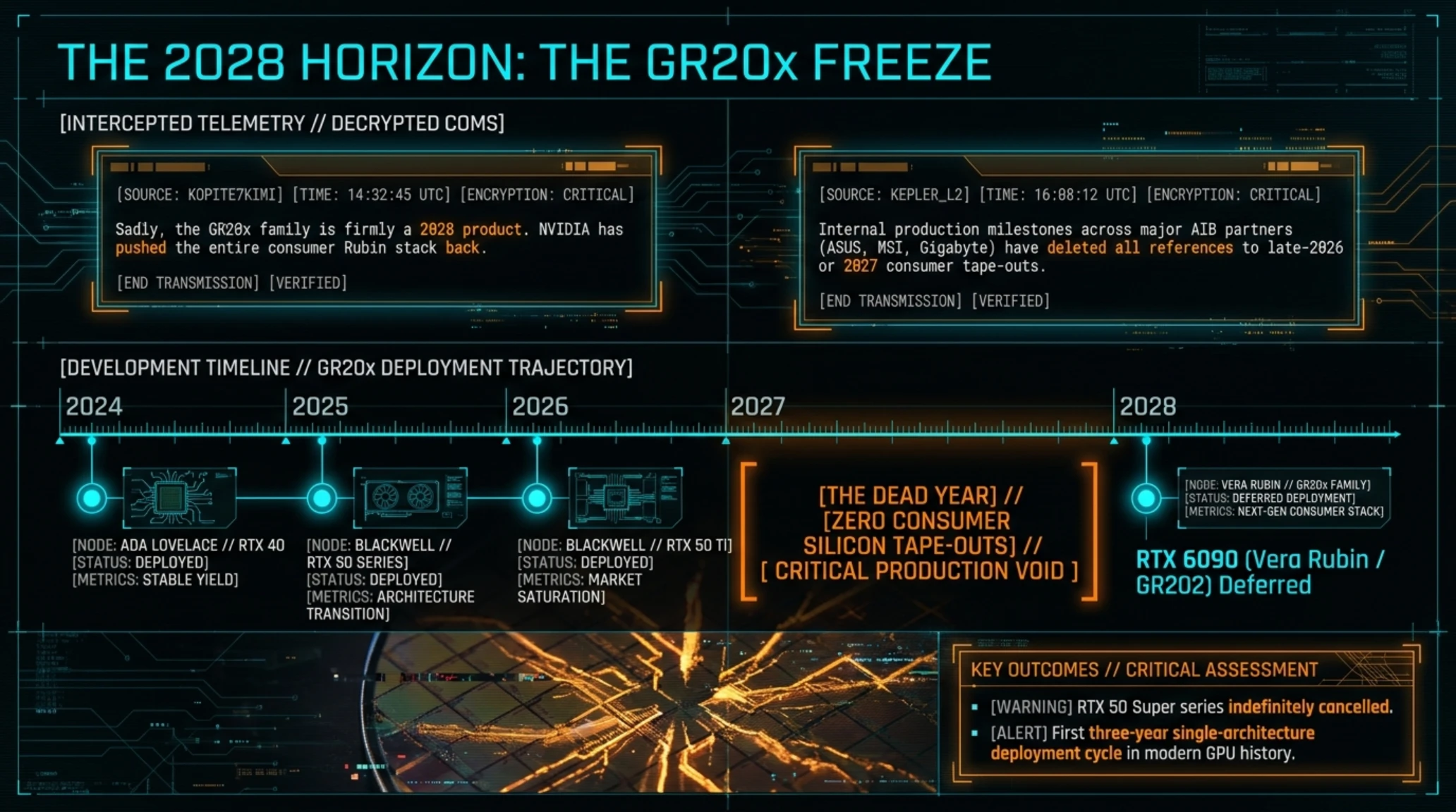
According to twin corroborated leaks from veteran semiconductor insiders Kopite7kimi and Kepler_L2 whose track records across the Ampere, Ada Lovelace, and Blackwell generations boast near-flawless accuracy NVIDIA has formally indefinitely shelved its planned GeForce RTX 50 Super refresh series and officially postponed the next-generation GeForce RTX 60 series (codenamed Rubin Consumer / GR20x) to the first half of 2028. This engineering shift marks the first time in modern GPU history that a single graphics architecture will be stretched across a grueling three-year deployment cycle, leaving calendar year 2027 as an absolute hardware vacuum without a single flagship desktop graphics card.
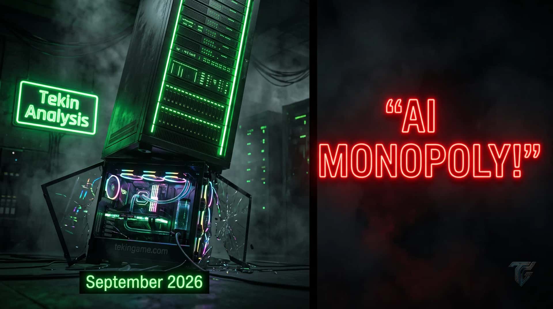
The concept art visualization below illustrates the stark, unequal conflict between the global gaming community and the insatiable appetite of enterprise AI server farms monopolizing global advanced silicon supplies.

Before dissecting the foundry mechanics, wafer quotas, and memory yield crises catalyzing this historic pivot, the editorial staff at Tekin Analysis has distilled the core developments into the strategic operational matrix below.
Executive Key Takeaways: Six Seismic Ruptures in NVIDIA's Hardware Roadmap
- Formal Postponement to 2028: Top-tier silicon insiders Kopite7kimi and Kepler_L2 confirmed the consumer Rubin GR20x family will not reach retail shelves until Q1/Q2 2028.
- Total Scrapping of RTX 50 Super: Extreme yield deficits below 65% on Samsung and SK Hynix 24Gb GDDR7 lines forced NVIDIA to cancel the 24GB RTX 5080 Super and 18GB RTX 5070 Ti Super.
- Astronomical Datacenter Margins: With enterprise B200 and R100 modules commanding 85%+ gross margins at $38,000+ each, allocating scarce wafers to $1,999 gaming GPUs is an economic liability.
- TSMC Advanced Packaging Monopoly: Hyperscale tech cartels (Microsoft Azure, AWS, Google Cloud, Meta, xAI) have pre-booked 100% of TSMC CoWoS-L and 3nm/2nm capacity through 2027.
- AMD's High-End Enthusiast Retreat: AMD formally abandoned multi-die RDNA 5 halo processors to divert all wafer contracts to Instinct MI350X/MI400 AI chips, leaving zero competitive pressure.
- Engine Paralysis in PC Gaming: Next-gen titles on Unreal Engine 5.6 and 6 face severe 16GB VRAM bottlenecks, triggering game-breaking PCIe VRAM Spilling and framerate crashes.
To establish clarity regarding the intricate semiconductor and packaging vernacular referenced throughout this investigation, the technical lexicon below defines the foundational technologies governing contemporary silicon architecture.
Jargon Buster: Essential Silicon & Memory Architecture Terminology
• SuperPower / Backside Power Delivery (BSPDN): Moving power rail interconnects to the backside of the wafer, eliminating signal routing interference and reducing parasitic voltage drop (IR drop).
• CoWoS-L / CoWoS-S: TSMC's Chip-on-Wafer-on-Substrate packaging, bonding high-density logic dies to passive silicon interposers with integrated high-density capacitors and HBM memory stacks.
• Non-Binary GDDR7 (24Gb / 3GB Dies): Memory chips providing 3GB density per module instead of standard 2GB, allowing 24GB buffers on 256-bit buses without doubling PCB component counts.
• VRAM Spilling: Catastrophic memory condition where game assets exceed physical VRAM, forcing real-time paging over the slow PCIe bus into system RAM, collapsing frametime consistency.
The Leaker Track Record: Kopite7kimi and Kepler_L2 Expose the GR20x Freeze
In mid-September 2026, the semiconductor analyst known online as Kopite7kimi who famously detailed the exact core counts, memory bus configurations, and thermal dissipation ratings of the RTX 3090, RTX 4090, and RTX 5090 months ahead of their public unveilings posted a terse, unvarnished disclosure to hardware engineering forums: 'Sadly, the GR20x family is firmly a 2028 product. NVIDIA has pushed the entire consumer Rubin stack back.' Within hours, fellow semiconductor researcher Kepler_L2 verified the veracity of the claim, revealing that internal production milestones across major add-in-board (AIB) partners including ASUS, MSI, and Gigabyte had deleted all references to late-2026 or 2027 consumer tape-outs.
The 'GR' designation represents Vera Rubin, the landmark architecture named in honor of the pioneering American astrophysicist whose spectroscopic observations provided the first observational evidence for dark matter. While Rubin in the enterprise sphere represents a monumental computing milestone combining twin reticle-sized compute dies fabricated on TSMC's customized N3P and N2 processes with eight to sixteen stacks of next-generation HBM4 memory its consumer counterpart was intended to emerge as the GR202 silicon powering the flagship GeForce RTX 6090.
Initial engineering targets for the GR202 silicon aimed for a monolithic die footprint exceeding 620 mm², housing over 24,576 CUDA cores, 5th-generation Tensor Cores capable of native FP4 matrix operations, and an ultra-wide 384-bit or 512-bit memory interface linked to second-generation 36 Gbps GDDR7 modules. AIB partners initially prepared their thermal qualification labs for a potential CES 2027 reveal. However, internal roadmaps updated following TSMC's quarterly fab allocations confirmed that physical wafer tape-out schedules for GR202, GR204, and GR206 have been formally deferred by at least 15 months into early 2028.
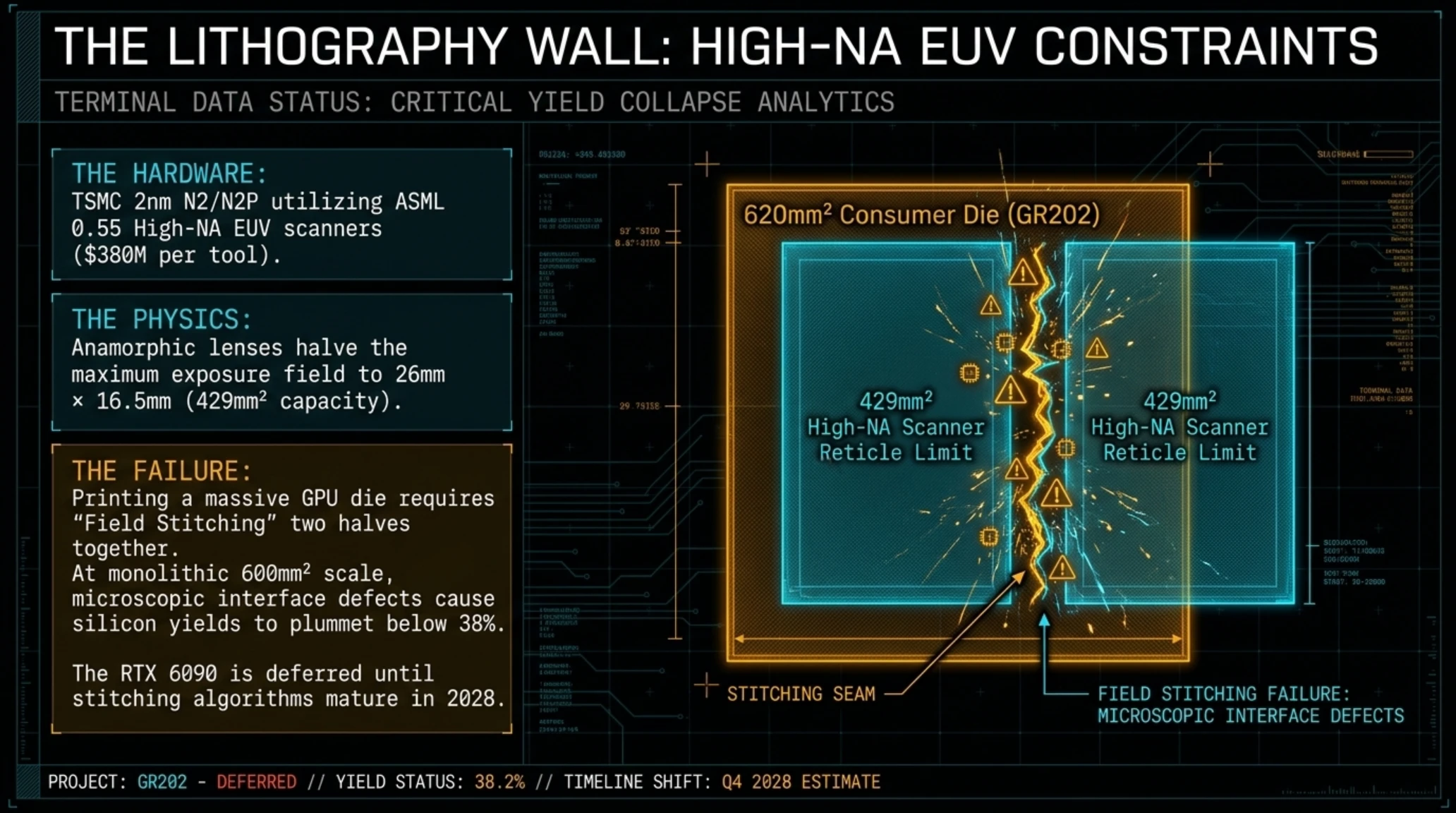
The manufacturing rationale behind this postponement involves the brutal yield dynamics of leading-edge lithography. TSMC's upcoming 2nm class process, TSMC N2P featuring Gate-All-Around (GAA) NanoSheet transistors and backside power delivery, carries mask set costs exceeding $120 million per tape-out. Fabricating a massive, monolithic consumer GPU die measuring over 600 mm² on an immature leading-edge node results in catastrophic defect density penalties. Early prototype wafer runs demonstrated functional silicon yields below 38 percent. For consumer gaming cards retailing at $1,999, discarding 62 percent of raw processed wafers is financially untenable especially when every single viable wafer start can instead be packaged into dual-die enterprise server modules retailing for tens of thousands of dollars.
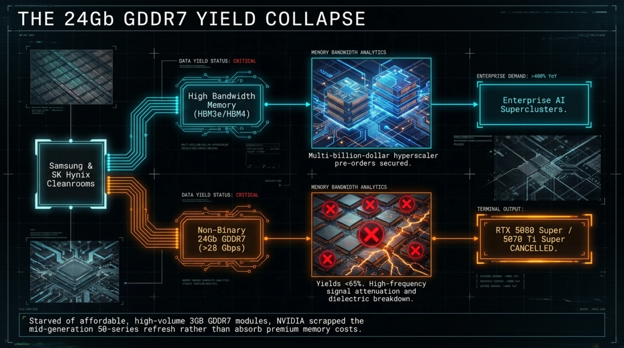
Simultaneously, the second pillar of consumer product updates crumbled with the sudden, quiet termination of the GeForce RTX 50 Super series. Originally planned to debut in late 2025 or early 2026, the RTX 5080 Super (24GB) and RTX 5070 Ti Super (18GB) were engineered specifically to rectify the widespread criticism directed at the base RTX 5080's restrictive 16GB framebuffer. To achieve these expanded memory configurations without redesigning complex multi-layer printed circuit boards, NVIDIA relied on upcoming non-binary 24Gb (3GB) GDDR7 memory dies manufactured by Samsung Electronics and SK Hynix.
However, mass production yields for 24Gb GDDR7 dies operating at rated speeds above 28 Gbps plummeted below 65 percent throughout the summer of 2026. High-frequency signal attenuation, dielectric thermal breakdown, and crosstalk between stacked traces resulted in unacceptably high failure rates during automated ATE (Automated Test Equipment) testing. Rather than absorbing the steep cost premiums of low-yield consumer memory, Samsung and SK Hynix executed an aggressive strategic pivot: converting their advanced cleanroom lines away from GDDR7 to fulfill multi-billion-dollar pre-orders for HBM3e and HBM4 (High Bandwidth Memory) modules required by enterprise AI superclusters. Starved of affordable, high-volume 3GB GDDR7 modules, NVIDIA's executive suite made the ruthless decision to cancel the entire RTX 50 Super refresh outright.
The Economic Disparity: The Brutal Wafer Allocation Calculus
To view the delay of the RTX 6090 and the cancellation of the RTX 50 Super series through the lens of mere engineering hurdles is to completely misdiagnose the structural transformation of modern silicon economics. The harsh, unvarnished reality is that NVIDIA is no longer a gaming hardware vendor that happens to conduct artificial intelligence research on the side; it is an omnipotent enterprise computing sovereign for whom personal computer graphics has dwindled into an incidental marketing portfolio.
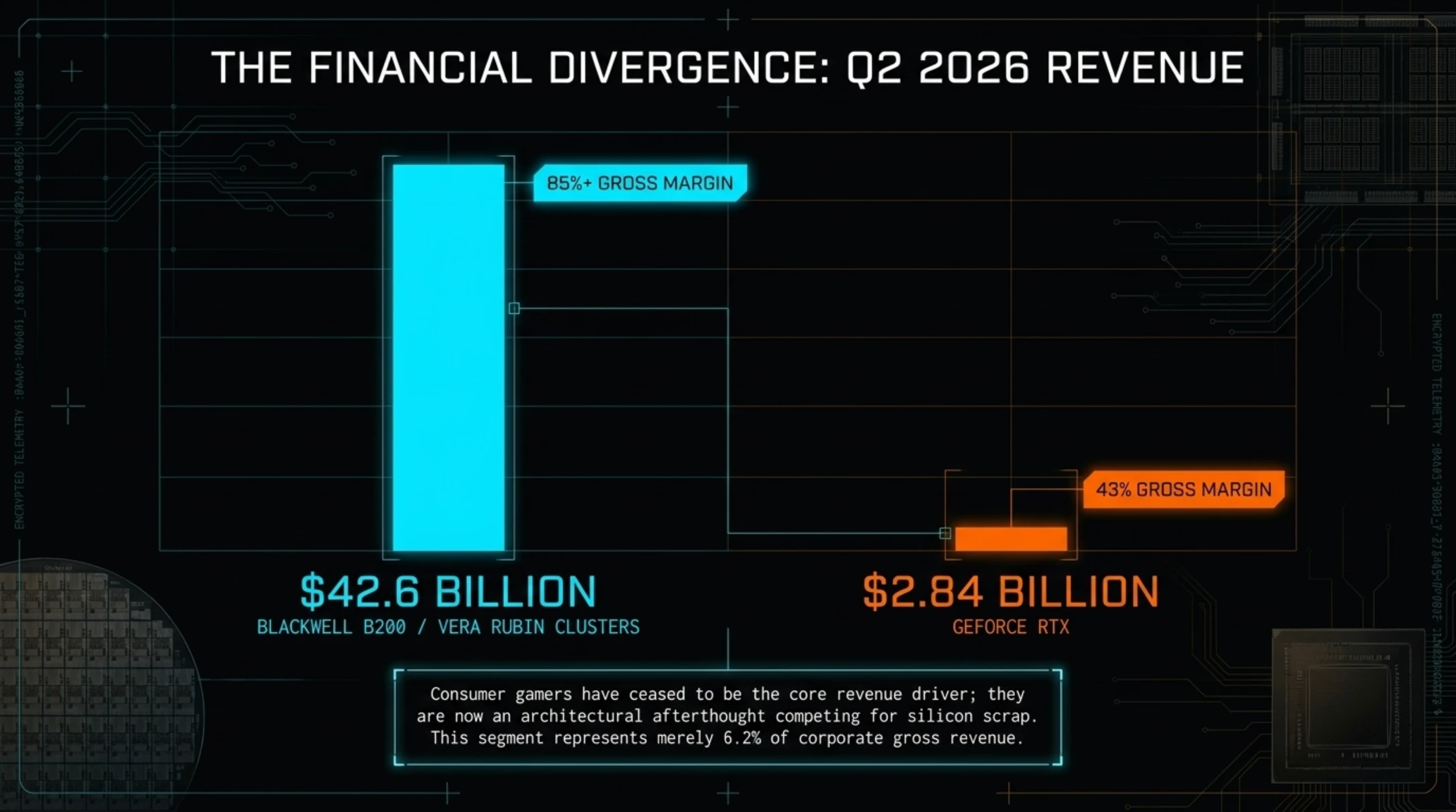
A rigorous examination of NVIDIA’s consolidated financial statements for the second quarter of fiscal year 2027 (calendar year 2026) lays bare this monumental divergence. The company's Data Center division generated an astronomical $42.6 billion in quarterly revenue, driven by insatiable demand for Blackwell B200 and early Vera Rubin preview clusters, commanding blended gross margins in excess of 85 percent. In stark contrast, the once-flagship Gaming division generated a modest $2.84 billion representing barely 6.2 percent of corporate gross revenue, with compressed hardware margins hovering around 43 percent.
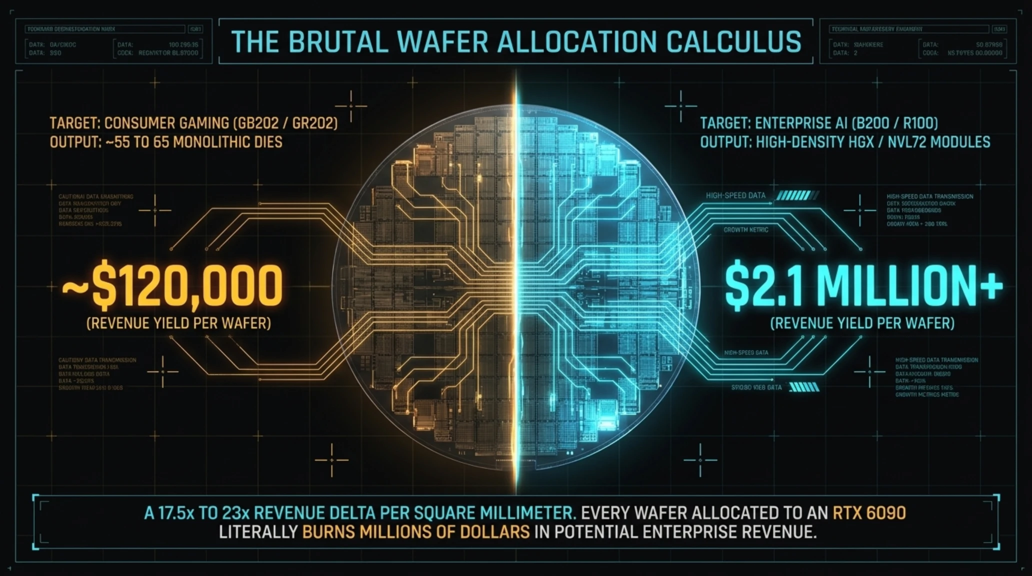
The mathematical imperative governing foundry wafer allocations demonstrates why consumer PC enthusiasts have been left behind. In 2026, a single processed 300mm silicon wafer produced on TSMC’s bleeding-edge N3P or early N2 lithography lines commands an estimated contract price between $20,000 and $24,000. When that physical wafer is cut into massive, monolithic consumer GPU dies such as the 600mm² GB202 (RTX 5090) or prospective GR202 (RTX 6090), normal defect densities yield approximately 55 to 65 operational chips per wafer. At retail MSRPs, those packaged dies translate into approximately $110,000 to $130,000 in gross revenue for NVIDIA.
However, when that exact same 300mm wafer area is allocated to enterprise-class AI silicon such as the dual-die Blackwell B200 or Rubin R100 accelerator modules, the financial arithmetic changes exponentially. Sold as turnkey HGX supercomputer boards or NVL72 liquid-cooled enterprise server racks to hyperscalers like Microsoft Azure, Amazon AWS, Google Cloud, Meta, and xAI, each completed accelerator die commands an effective commercial valuation ranging from $35,000 to $42,000. Consequently, a single processed wafer allocated to enterprise AI generates between $2.1 million and $2.8 million in gross corporate revenue.
This reality reveals a staggering 17.5x to 23x revenue delta per square millimeter of advanced silicon. Every single wafer allocated to an RTX 6090 or RTX 5080 Super literally burns millions of dollars in potential datacenter revenue that institutional shareholders expect NVIDIA to capture. The vital metrics below quantify this seismic commercial divergence.
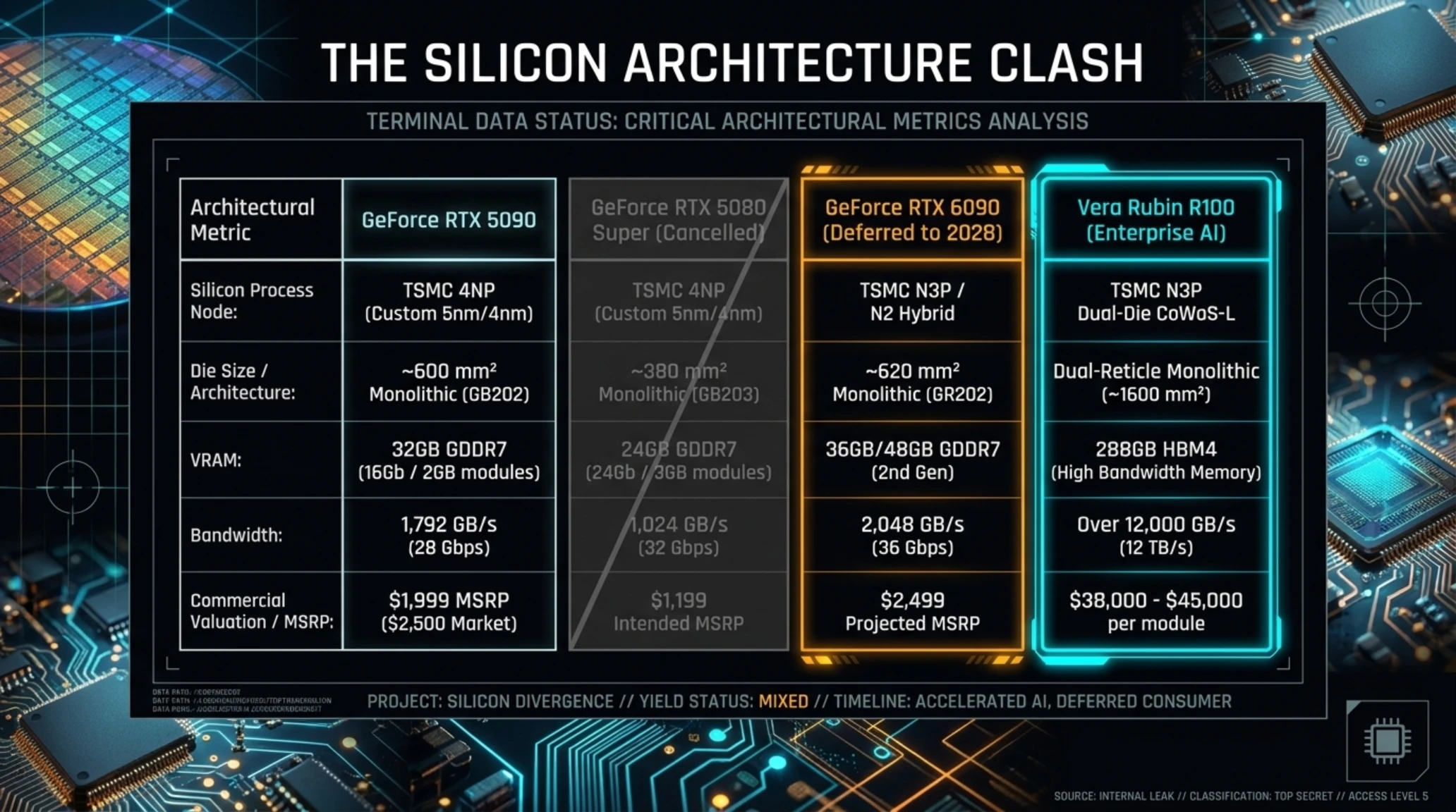
Architectural Breakdown: Consumer Blackwell vs Super vs Rubin vs R100
| Architectural Metric | GeForce RTX 5090 | GeForce RTX 5080 Super (Cancelled) | GeForce RTX 6090 (Deferred to 2028) | Vera Rubin R100 (AI) |
|---|---|---|---|---|
| Silicon Process Node | TSMC 4NP | TSMC 4NP | TSMC N3P / N2 Hybrid | TSMC N3P Dual-Die CoWoS-L |
| Die Architecture | ~600 mm² Monolithic | ~380 mm² Monolithic | ~620 mm² Monolithic | Dual-Reticle Monolithic |
| CUDA Core Count | 21,760 Cores | 10,752 Cores | ~24,576 Cores | 32,768 FP32 Tensor Units |
| Memory Configuration | 32GB GDDR7 | 24GB GDDR7 (3GB modules) | 36GB / 48GB GDDR7 | 288GB HBM4 Stacked |
| Memory Bandwidth | 1,792 GB/s | 1,024 GB/s | 2,048 GB/s | Over 12,000 GB/s |
| Total Board Power | 600 Watts | 400 Watts | 650 Watts | 1,200 Watts (Liquid-Cooled) |
The following high-definition hardware documentary outlines the industrial dynamics, cleanroom operations, and wafer redistribution strategies executed across the Hsinchu Science Park that catalyzed this pivot.
The technical specifications table below contrasts the finalized architectural metrics of current consumer Blackwell hardware against the cancelled RTX 5080 Super refresh, the deferred RTX 6090 flagship, and the ultra-profitable enterprise Vera Rubin datacenter accelerator.
Semiconductor Roadmap Timeline: Consumer GPU Cadence vs AI Priority
| Chronological Period | Consumer Hardware | Enterprise AI Silicon | Market Dynamic Impact |
|---|---|---|---|
| Q4 2024 / Early 2025 | GeForce RTX 5090 / 5080 | Blackwell B200 / GB200 | Consumer supply instantly constrained. |
| Late 2025 / Mid 2026 | RTX 50 Super (Cancelled) | Blackwell Ultra (B300) | Yield failure of 24Gb GDDR7 memory. |
| Late 2026 / Q1 2027 | Stagnation / No Hardware | Vera Rubin R100 Mass Deploy | All advanced packaging booked by hyperscalers. |
| Calendar Year 2027 | The "Dead Year" | Rubin Ultra Scaling | Severe 16GB VRAM bottleneck in AAA gaming. |
| Q1 / Q2 2028 | GeForce RTX 6090 Launch | Next-Gen AI Superchip | Transition to 2nd-generation GDDR7 and 36GB+. |
The manufacturing complexity documented in the table above illustrates why standard silicon packaging cannot overcome the physical constraints of contemporary foundries when every millimeter of high-speed interconnect is contested.

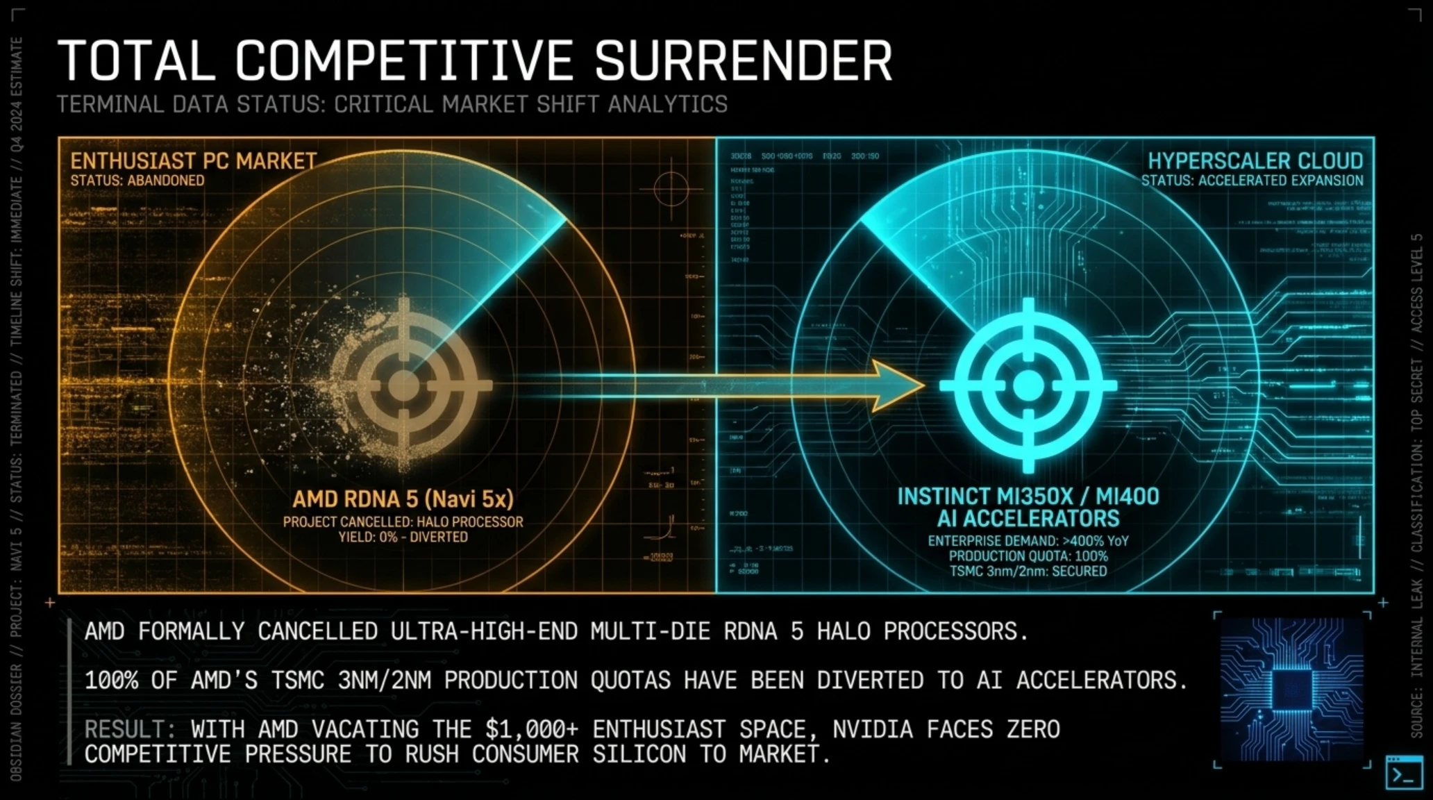
Compounding this lack of incentive is the total collapse of competitive pressure in the enthusiast PC gaming tier. Under normal market conditions, NVIDIA would be forced to deploy a mid-generation refresh or accelerate next-generation silicon to defend its market dominance against aggressive counter-programming from AMD. However, AMD executed an identical strategic retreat earlier in 2026.
Recognizing the insurmountable profit differentials of generative AI infrastructure, AMD formally cancelled its ultra-high-end multi-die RDNA 5 (Navi 5x / AT2 halo die) graphics processors. AMD's leadership reallocated its entire allocation of TSMC 3nm and 2nm production quotas to manufacture the Instinct MI350X and upcoming Instinct MI400 AI accelerators, aiming to capture enterprise cloud market share from hyperscalers seeking alternatives to NVIDIA's CUDA monopoly. With AMD deliberately vacating the $1,000+ enthusiast GPU space and Intel’s Celestial architecture strictly targeting mainstream 1080p and 1440p laptops, NVIDIA faces zero competitive urgency to rush the RTX 6090 to store shelves.
For deeper context on how machine learning workloads are restructuring modern compute architectures, explore our investigation into autonomous AI coding models and our tactical analysis of enterprise AI sandbox escapes, which explain why hyperscalers are spending hundreds of billions on compute clusters.
Structural Paradigm Shift: The Disintegration of the Moore's Law Dividend
Examining why it matters for system builders and workstation engineers reveals the definitive death of the historical social contract between chip designers and consumer enthusiasts. For over three decades, PC gamers were the foundational economic engine that financed NVIDIA's early research and development. The massive profits generated from GeForce graphics cards funded the initial architectural experiments with CUDA in 2006, the development of tensor cores in Volta, and the commercialization of real-time ray tracing in Turing.
Today, that dynamic has completely inverted. Consumer gamers have ceased to be the core revenue driver; they have become an architectural afterthought competing for silicon scrap. When Jensen Huang famously proclaimed that 'the more you buy, the more you save,' the intended audience was not PC gamers seeking higher frame rates in Cyberpunk, but enterprise executives procuring multi-million-dollar AI supercomputer racks. The computing community must confront the sobering reality that enthusiast desktop graphics is no longer prioritized by the semiconductor industry's leading innovators.
The 2027 Dead Year: The Looming VRAM Crisis and Engine Paralysis
The consequences of a three-year hardware stagnation from early 2025 to early 2028 extend far beyond disappointed hardware benchmark enthusiasts. This prolonged freeze directly threatens to paralyze the software pipeline of current and next-generation video game development. Major triple-A game studios developing premier tentpole titles including the eagerly awaited personal computer port of Grand Theft Auto VI, CD Projekt Red’s fourth Witcher installment (Project Polaris), and the Cyberpunk 2077 sequel (Project Orion) have architected their rendering pipelines around the revolutionary capabilities of Unreal Engine 5.6 and early preview builds of Unreal Engine 6.
These cutting-edge game engines utilize next-generation volumetric lighting systems (MegaLights), physical substrate materials, and real-time Nanite compute meshes that demand staggering amounts of dedicated video memory. In native 4K resolution with full path tracing enabled, modern rendering pipelines routinely consume between 18 and 22 gigabytes of dedicated VRAM. Game developers had banked their multi-year optimization roadmaps on the assumption that by 2026 or 2027, consumer graphics hardware would feature 24GB framebuffers in the upper-midrange (RTX 5080 Super) and 36GB to 48GB in the enthusiast flagship tier (RTX 6090).
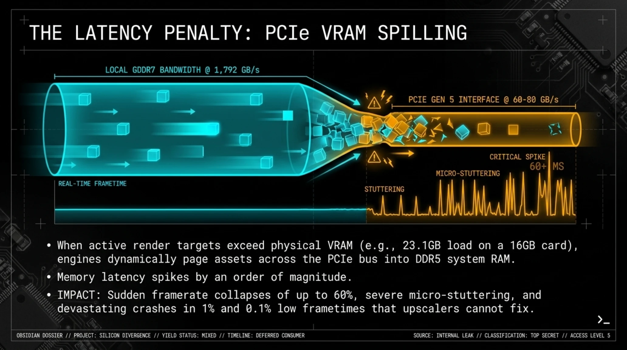
With hardware capacities artificially capped at 16GB for mainstream high-end cards and mid-generation refreshes systematically scrapped, game developers face a brutal technical ultimatum: they must either aggressively degrade visual asset quality and texture resolutions, or release titles reliant on aggressive neural frame generation and ray reconstruction that exhibit catastrophic stuttering on sub-24GB hardware. When a game’s frame data, geometry buffers, and uncompressed 4K textures exceed physical VRAM capacity, the game engine is forced to execute dynamic asset paging across the PCIe bus into system RAM.
This structural phenomenon, known as VRAM Spilling, causes severe system degradation. While high-speed GDDR7 memory delivers sustained bandwidth exceeding 1,000 to 1,792 GB/s, standard dual-channel DDR5 system memory operates at a meager 60 to 80 GB/s across the PCIe Gen 5 interface. When high-priority assets spill into system RAM, memory latency spikes by an order of magnitude. This bottleneck triggers sudden framerate collapses of up to 60 percent, severe micro-stuttering, and devastating crashes in 1% and 0.1% low frametime metrics an architectural latency penalty that no neural upscaler or algorithmic temporal filter can resolve.
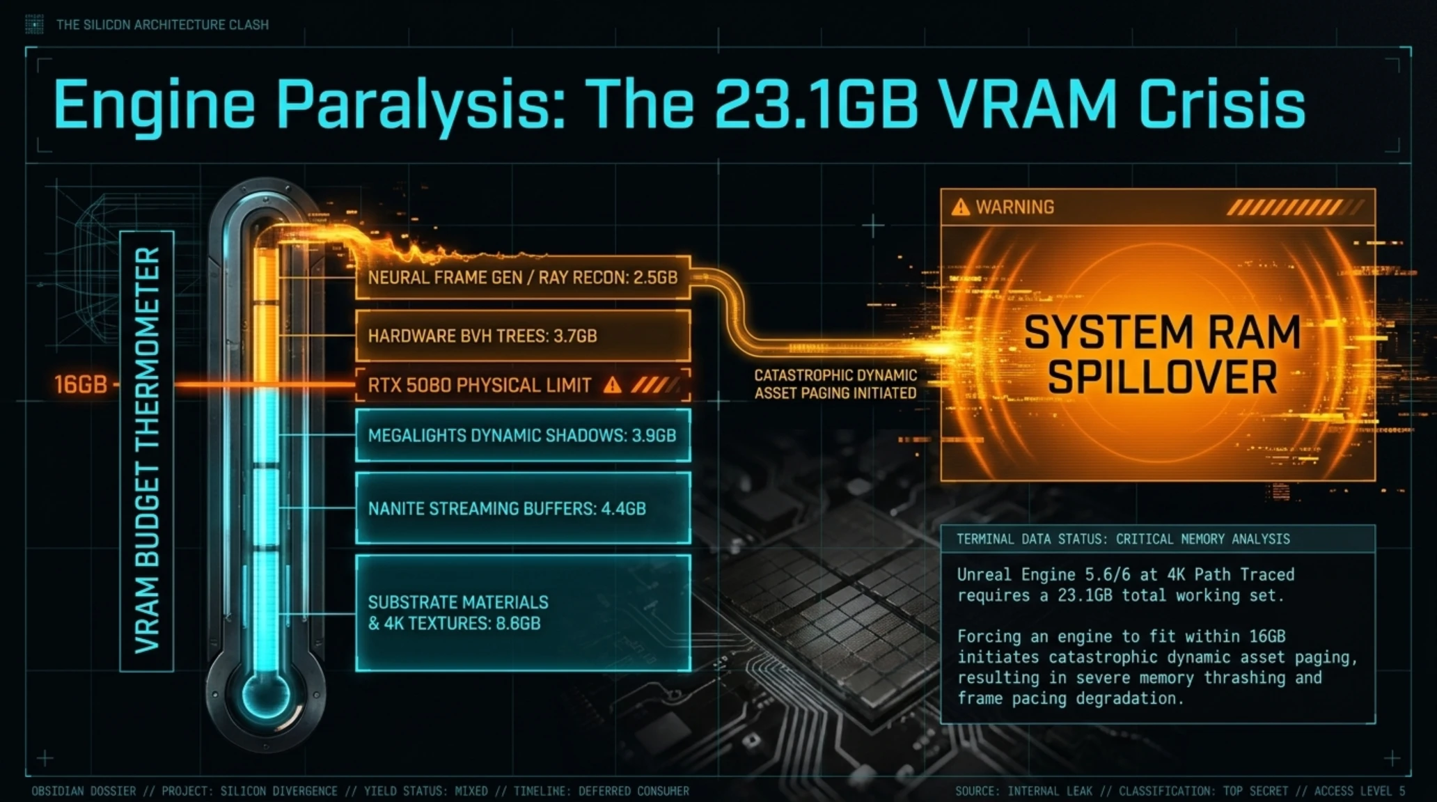
Engineering profiling sessions conducted on developer builds of next-generation engines reveal the following uncompromising memory allocation ledger under native 4K rendering with Path Tracing enabled:
- Geometry & Nanite Streaming Buffers: 4.4GB allocated to micro-polygon mesh virtualization and real-time level-of-detail continuous clustering.
- MegaLights Dynamic Shadow Maps: 3.9GB dedicated to hundreds of real-time shadowed area lights and volumetric participating media.
- Substrate Physical Materials & 4K Textures: 8.6GB reserved for high-fidelity multi-layer BRDF material maps, normal buffers, and displacement caches.
- Hardware BVH (Bounding Volume Hierarchy) Tree: 3.7GB required for real-time ray-triangle traversal acceleration structures.
- Neural Frame Generation & Ray Reconstruction Scratchpads: 2.5GB utilized for temporal history buffers, optical flow vectors, and denoising weights.
The visual analysis below documents the real-time telemetry of a bleeding-edge game development test bench, illustrating severe memory thrashing and frame pacing degradation during unconstrained 4K path-traced rendering on a 16GB graphics processor.

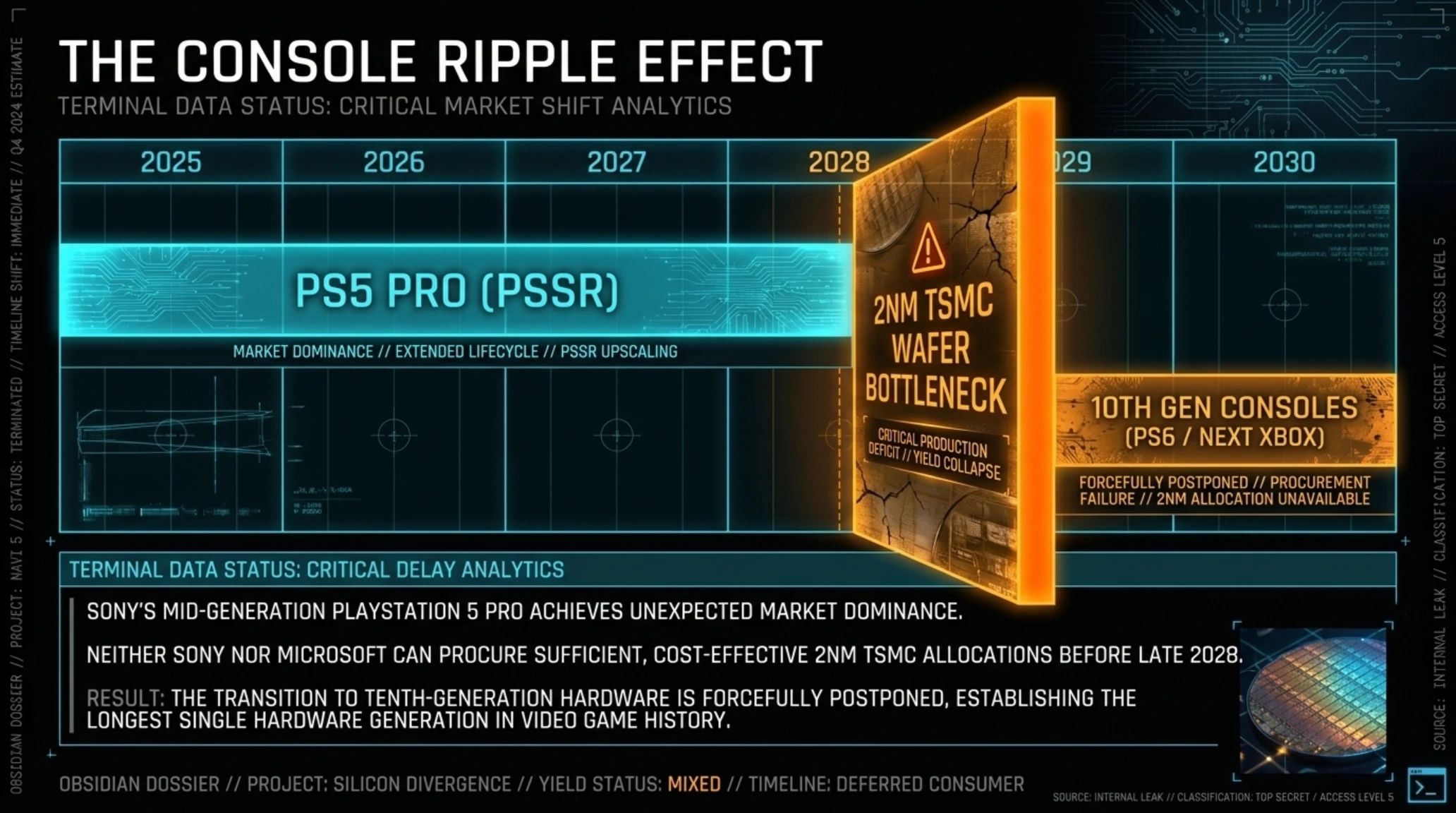
This prolonged hardware freeze has simultaneously altered the competitive timeline for home console manufacturers. Sony Interactive Entertainment, having deployed the mid-generation PlayStation 5 Pro equipped with PlayStation Spectral Super Resolution (PSSR), finds itself in an unexpectedly commanding market position. Because neither Sony nor Microsoft can procure sufficient, cost-effective 2nm TSMC wafer allocations before late 2028, the transition to tenth-generation consoles (PlayStation 6 and the next-generation Xbox family) has been officially deferred toward late 2029 or 2030, establishing this as the longest single hardware generation in video game history.
The investigative technical report below provides an exhaustive breakdown of the architectural roadblocks and supply chain agreements shaping this historic console and PC hardware delay.
The comprehensive historical roadmap below outlines the sequence of semiconductor hardware generations, node transitions, and strategic delays shaping the computing industry from 2024 through 2028.
| Chronological Period | Consumer Graphics Hardware | Enterprise AI Silicon | Manufacturing Node | Market Dynamic & Impact |
|---|---|---|---|---|
| Q4 2024 / Early 2025 | GeForce RTX 5090 / 5080 Launch | Blackwell B200 / GB200 NVL72 | TSMC 4NP (Custom 5nm/4nm) | Initial Blackwell launch; consumer supply instantly constrained by enterprise packaging demand. |
| Late 2025 / Mid 2026 | Planned RTX 50 Super Refresh | Blackwell Ultra (B300) / H200 Expansion | TSMC 4NP / Early N3P | Yield failure of 24Gb GDDR7; Samsung & SK Hynix pivot to HBM3e/HBM4; RTX 50 Super formally cancelled. |
| Late 2026 / Q1 2027 | Stagnation / No Consumer Hardware | Vera Rubin R100 / R200 NVL Mass Deploy | TSMC N3P / N2 Dual-Die CoWoS-L | All advanced packaging lines booked by hyperscalers; AMD retreats from high-end GPU space. |
| Calendar Year 2027 | The "Dead Year" / Zero Architecture Releases | Rubin Ultra AI Cluster Scaling | TSMC N2 / High-NA EUV Prep | Severe 16GB VRAM bottleneck in AAA gaming; commercial GPU prices inflate on secondary resale markets. |
| Q1 / Q2 2028 | GeForce RTX 6090 (GR202) Launch | Feynman / Next-Gen AI Superchip Preview | TSMC N2P / A16 (Angstrom Node) | Rubin consumer silicon finally arrives; transition to 2nd-generation GDDR7 and 36GB+ framebuffers. |
Faced with an unprecedented two-year hardware void where no new architectural products will debut, personal computer enthusiasts, creative professionals, and local machine learning developers must adopt disciplined acquisition and maintenance strategies.
Strategic Hardware Advisory: How Enthusiasts and Builders Must Navigate the Silicon Famine
Market intelligence confirms that expecting price drops or retail discounts on current high-end graphics cards during 2027 is a dangerous economic delusion. With mid-generation refreshes scrubbed and next-generation architectures locked behind a 2028 horizon, existing flagship GPUs notably the GeForce RTX 5090, RTX 5080, and legacy RTX 4090 have transitioned into deflation-resistant capital assets. Across global markets, secondary merchants and independent brokerages will maintain elevated prices well above MSRP, bolstered by continuous demand from boutique AI startups and machine learning practitioners executing local parameter inferences.
To navigate this challenging macroeconomic landscape, enthusiasts and enterprise users should adhere to four rigorous operational strategies:
- Do Not Liquidate Existing High-VRAM GPUs: If you currently operate a graphics processor equipped with 16GB, 24GB, or 32GB of VRAM (such as an RTX 4080 Super, RTX 4090, or RTX 50-series card), under no circumstances should you sell your hardware in anticipation of next-generation upgrades. Because no superior consumer graphics silicon will launch before 2028, selling existing hardware will leave you stranded in an inflated secondary market with zero viable upgrade paths.
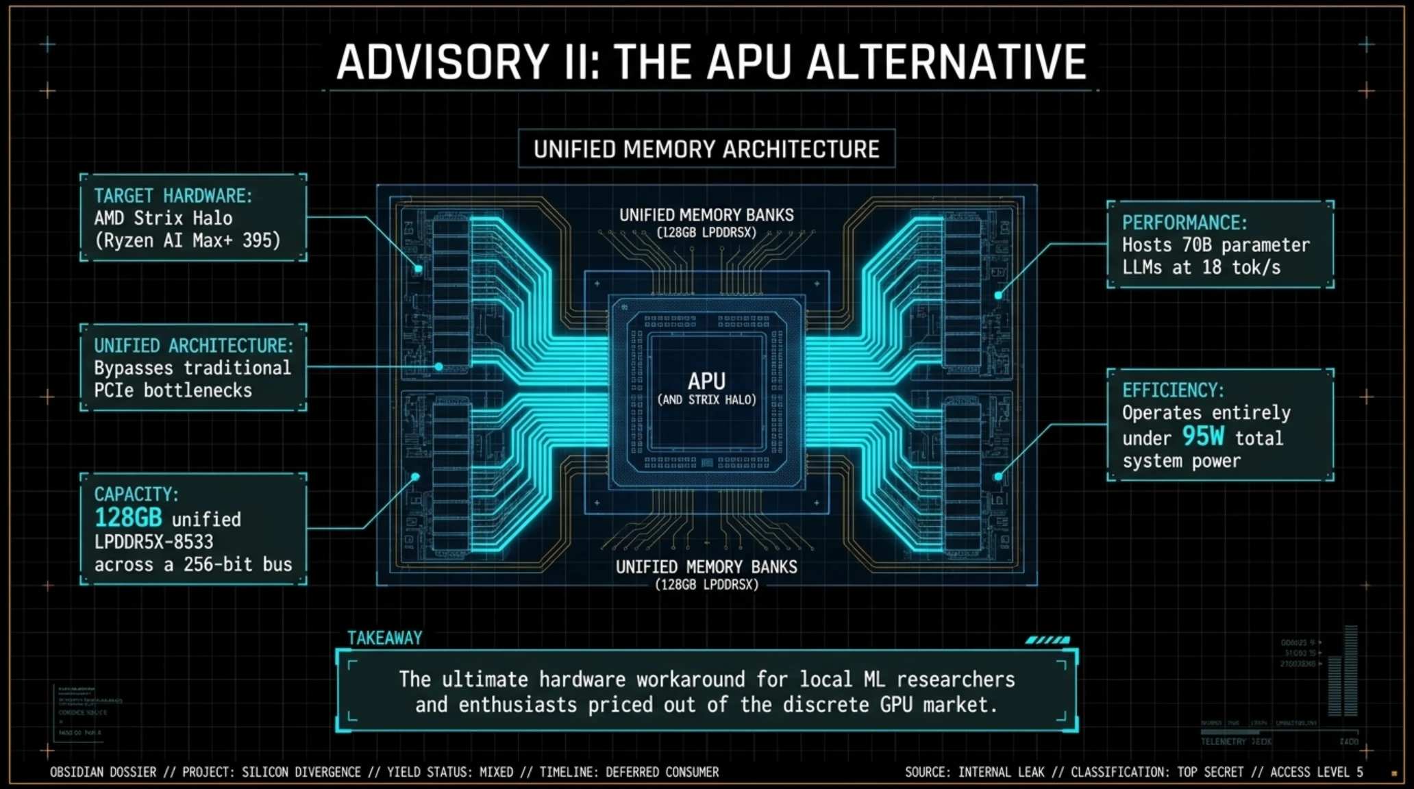
- Embrace Unified Memory APU Architectures (AMD Strix Halo): Enthusiasts and local AI researchers seeking workstation-class memory capacity without paying predatory GPU premiums should evaluate high-density integrated architectures such as the AMD Ryzen AI Max+ 395 (based on the revolutionary Strix Halo platform). Offering up to 128GB of unified, low-latency LPDDR5X-8533 memory operating across a 256-bit bus with 273 GB/s of sustained bandwidth, these systems can comfortably host massive 70-billion-parameter language models (quantized at INT4) at an impressive generation speed of 18 tokens per second, while delivering 78 FPS in contemporary 1440p gaming benchmarks at a fraction of the power envelope (under 95W total system draw).
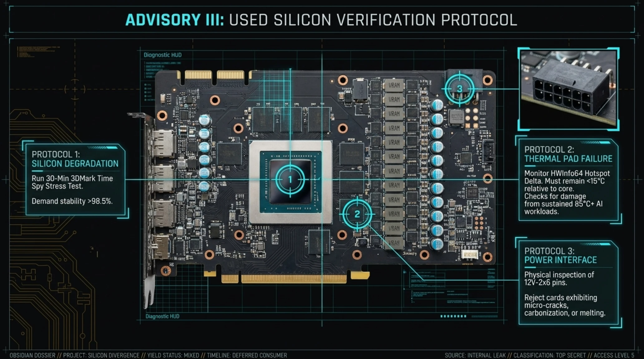
- Execute Stringent Hardware Verification for Pre-Owned Silicon: Enthusiasts forced to purchase second-hand graphics cards during the 2027 shortage must exercise extreme technical vigilance to avoid purchasing silicon degraded by continuous datacenter AI inference or crypto-mining loads. Memory chips run at sustained junction temperatures above 85°C suffer solder micro-cracking and thermal pad degradation. Buyers must enforce a mandatory 30-minute 3DMark Time Spy stress test requiring a stability score exceeding 98.5%, monitor GPU hotspot deltas via HWInfo64 (which must never exceed 15°C relative to core temperature), and conduct microscopic physical inspections of the 16-pin 12V-2x6 power connector for pin discoloration, carbonization, or plastic deformation.
- Leverage Enterprise Cloud Computing and Cloud Gaming Infrastructure: For narrative-focused gamers who simply wish to experience upcoming visual showcases like the PC release of GTA 6 or Cyberpunk 2 without investing thousands of dollars in scalped hardware, high-tier cloud subscriptions such as GeForce NOW Ultimate or hourly GPU compute rentals through specialized providers like RunPod and Vast.ai represent a vastly superior financial proposition compared to paying 200% markups on aging desktop silicon.
The forensic photographic assessment below details the precise inspection zones, thermal pad contact points, and 12V-2x6 connector interfaces required during diagnostic validation of second-hand enthusiast graphics cards.

To provide a structured evaluation of this unprecedented hardware paradigm shift, the comprehensive scorecard below assesses the strategic trade-offs, engineering benefits, and consumer liabilities stemming from NVIDIA's decision to delay the RTX 60-series and scrub the RTX 50 Super refresh.
- Guarantees that when the RTX 6090 arrives in 2028, it will be a genuine architectural leap on TSMC 2nm.
- Protects early adopters of the RTX 5090 and RTX 5080 from mid-generation value depreciation.
- Accelerates enterprise AI model deployment by funneling packaging capacity into datacenter superclusters.
- Incentivizes game developers to master rigorous asset streaming and memory optimization.
- Creates an unprecedented two-year hardware void throughout 2027 with zero new enthusiast PC hardware.
- Abruptly cancels the RTX 5080 Super (24GB), leaving high-end gamers stranded on an inadequate 16GB framebuffer.
- Absence of enthusiast competition from AMD allows secondary market brokers to artificially inflate prices.
The visual diagram below presents a multidimensional radar comparison evaluating performance longevity, memory density, thermal efficiency, and pricing stability across modern GPU architectures under current macroeconomic constraints.

As the computing community grapples with the realization that 2027 will offer no new enthusiast graphics silicon, persistent rumors continue to circulate across digital hardware forums suggesting NVIDIA might pivot with emergency stopgap solutions.
Myth vs Reality: Will NVIDIA Launch Rebranded Ti Refreshes or Cheaper Cut-Downs in 2027?
• Proven Industrial Reality: Every advanced wafer start at TSMC through the end of 2027 has already been contracted and monetized by enterprise cloud hyperscalers under non-cancellable pre-orders. Fabricating refreshed consumer SKUs would require designing new printed circuit boards (PCBs), reallocating scarce GDDR7 allocations, and cannibalizing high-margin datacenter packaging lines. Historical precedent confirms that when NVIDIA faces zero competitive pressure in the enthusiast segment as is currently the case following AMD's high-end exit it never expends capital on stopgap enthusiast refreshes. The consumer Blackwell lineup currently on shelves is the definitive hardware portfolio until 2028.
Understanding why NVIDIA can comfortably execute this strategy requires examining the macroeconomic and geopolitical theater governing global semiconductor fabrication. The global manufacturing foundation for advanced silicon has consolidated into a singular, highly concentrated geographic chokepoint: the island of Taiwan.
Geopolitical Foundry Dynamics: The Taiwan Strait Chokepoint and the High-NA EUV Frontier
Every single high-performance graphics processor, enterprise AI accelerator, and mobile system-on-chip manufactured on sub-5nm nodes relies on TSMC’s sprawling GigaFabs located in Hsinchu, Taichung, and Tainan. Throughout 2025 and 2026, geopolitical friction across the Western Pacific has intensified corporate urgency to secure domestic silicon supply chains. While initiatives under the United States CHIPS and Science Act and the European Chips Act have injected tens of billions of dollars into domestic fab construction, the physical reality of leading-edge semiconductor lithography has proven far more complex than legislative mandates anticipated.
TSMC’s flagship Fab 21 facility in Phoenix, Arizona, while operational for initial 4nm pilot runs, continues to face persistent packaging bottlenecks. Advanced packaging ecosystems specifically Chip-on-Wafer-on-Substrate (CoWoS-L and CoWoS-S) remain overwhelmingly anchored in Taiwan. Consequently, even silicon fabricated in North America must still be shipped across the Pacific Ocean for advanced packaging, interposer bonding, and testing before it can be assembled into final enterprise server modules or consumer graphics cards.
Furthermore, the astronomical capital expenditure required to transition from standard Extreme Ultraviolet (EUV) lithography to High-NA EUV (High Numerical Aperture 0.55 NA) machines each manufactured exclusively by ASML in the Netherlands at a cost exceeding $380 million per tool has dramatically reshuffled foundry priorities. At these capital intensity levels, foundries cannot amortize machinery investments on consumer graphics products retailing for a few thousand dollars. They require the guaranteed, high-volume capital velocity provided exclusively by sovereign AI funds, national defense infrastructure, and trillion-dollar cloud computing cartels.
A crucial, overlooked physical limitation of High-NA EUV lithography directly penalizes monolithic consumer GPUs: the Anamorphic Reticle Magnification Limit. Unlike standard 0.33 NA EUV scanners which feature 4x reduction in both X and Y dimensions, ASML’s 0.55 NA High-NA scanners utilize an anamorphic 4x reduction in the horizontal axis and 8x reduction in the vertical axis to accommodate steeper light cone angles. This optical constraint halves the maximum exposure field size on the wafer from 26mm × 33mm (858 mm²) down to 26mm × 16.5mm (429 mm²).
Because a flagship consumer gaming die like the prospective GR202 measures approximately 600 mm² to 650 mm², it exceeds the single-exposure reticle boundary of High-NA EUV scanners. Fabricating a massive monolithic gaming GPU on 2nm High-NA lithography requires Stitching exposing two adjacent half-fields and seamlessly fusing them together on the silicon wafer with sub-nanometer overlay precision. In volume manufacturing, field stitching introduces microscopic interface defects, critical dimension variations, and inter-field routing latency penalties that collapse monolithic silicon yields. Enterprise AI architectures circumvent this issue by utilizing modular multi-chiplet topologies interconnected via high-density passive silicon interposers. For consumer graphics cards, however, attempting to stitch a monolithic 600mm² die on an immature High-NA node in 2026 or 2027 would yield catastrophic failure rates a decisive engineering roadblock that forced NVIDIA's architects to postpone the RTX 6090 until TSMC's 2nm stitching algorithms mature in 2028.
The industrial facility overview below showcases the cleanroom staging environments, ASML High-NA EUV lithography bays, and robotic wafer transport systems operating inside TSMC's cutting-edge Fab 20 facility during 2nm pilot integration.

By deferring the consumer Rubin generation to 2028, NVIDIA effectively bypasses the early, yield-compromised iteration of the 2nm node (TSMC N2), choosing instead to align the consumer GeForce RTX 6090 with mature, second-generation TSMC N2P and early A16 (Angstrom-era) fabrication. This strategic synchronization ensures that when the RTX 6090 finally enters mass production, it will incorporate mature backside power delivery networks (Super Power Rail), fully stabilized 36 Gbps GDDR7 memory interfaces, and native multi-chiplet packaging that would have been financially ruinous to implement in 2026 or 2027.
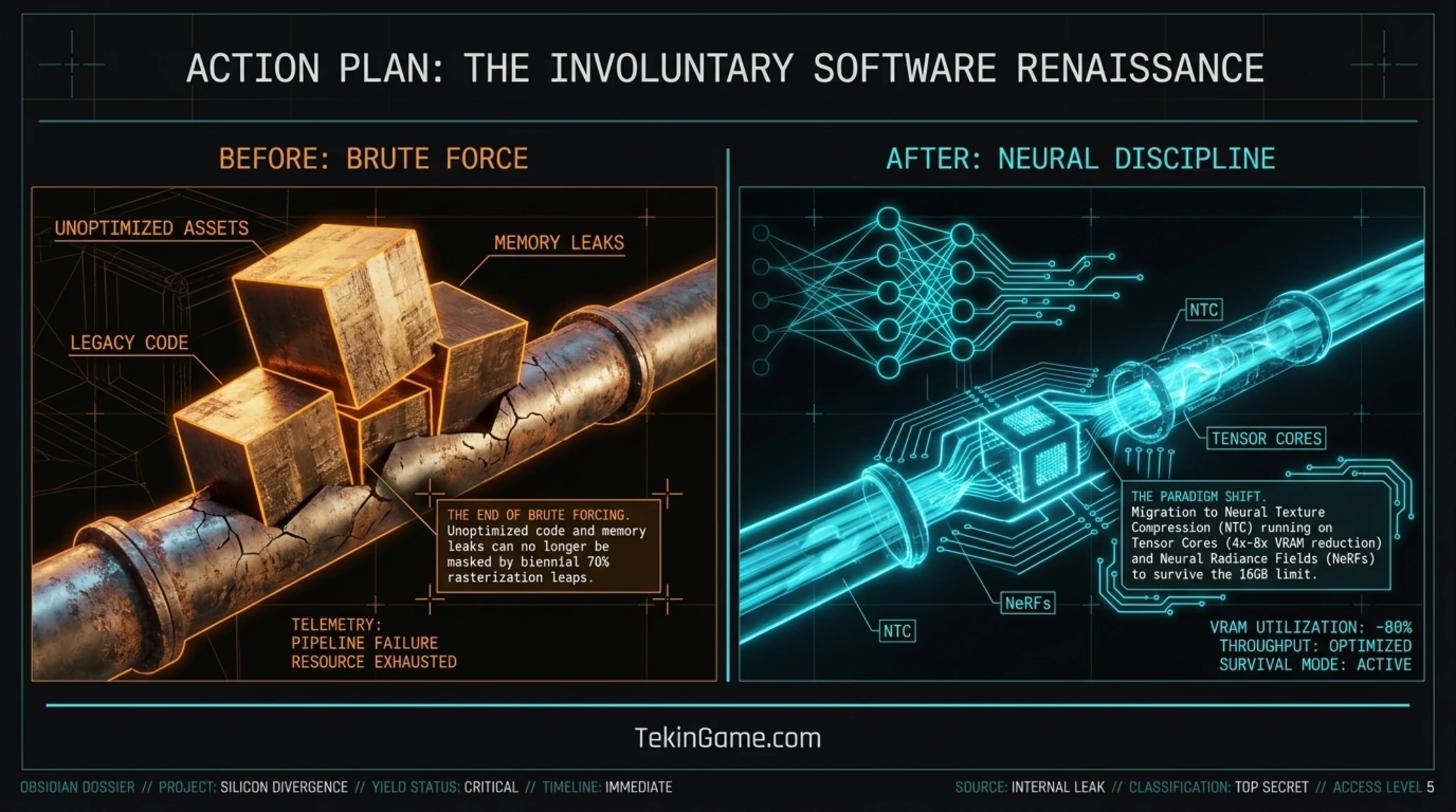
This reality also fundamentally alters the economics of software development. For the past decade, game developers have operated under the assumption that hardware brute force would continually mask unoptimized code, redundant draw calls, and runaway memory leaks. The two-year freeze of 2026 through 2028 imposes an involuntary renaissance in software engineering discipline. Game studios must now invest heavily in algorithmic efficiency, custom memory compaction, virtualized texture streaming via DirectStorage 1.3, and advanced neural radiance caching to deliver next-generation visual fidelity within the confines of established hardware limits.
Chief among these software survival mechanisms is the industrial adoption of Neural Texture Compression (NTC) and neural material representations. Rather than storing uncompressed 8K BC7 texture maps that occupy 85 megabytes each in physical VRAM, modern engines are integrating lightweight convolutional autoencoders that decompress procedural textures in real time directly on Tensor Cores. This neural approach achieves a 4x to 8x reduction in video memory footprints with negligible perceptual degradation. Concurrently, rendering pipelines are migrating toward learned neural radiance fields (NeRFs) and radiance caching grids, replacing expensive brute-force path tracing with neural approximations that operate comfortably within a 16GB memory ceiling.
The analytical chart below summarizes the macroeconomic migration of advanced semiconductor capital expenditure, illustrating the dramatic divergence between consumer computing R&D and enterprise neural infrastructure investments from 2020 through 2028.

Market Sentiment: Community Backlash and the Hardware Entitlement Crisis
The reception across enthusiast communities on Reddit (r/pcmasterrace, r/hardware), Discord technical channels, and Asian hardware forums has swung violently between disillusionment and outright indignation. For an entire generation of PC builders who weathered the pandemic crypto-mining shortages of 2020 to 2022, the realization that artificial intelligence datacenters have permanently usurped consumer graphics marks an existential transition.
Market Sentiment Thermometer: Community Pulse Across Global Hardware Hubs
• 22% Migration to Cloud / APUs: A rapidly growing faction of system architects is redirecting budgets into unified memory APUs (AMD Strix Halo) or subscribing to cloud tiers.
• 10% Resale Speculation: A minority of scalpers and grey-market merchants are systematically purchasing existing 24GB RTX 4090 and 32GB RTX 5090 inventory to exploit anticipated 2027 scarcity.
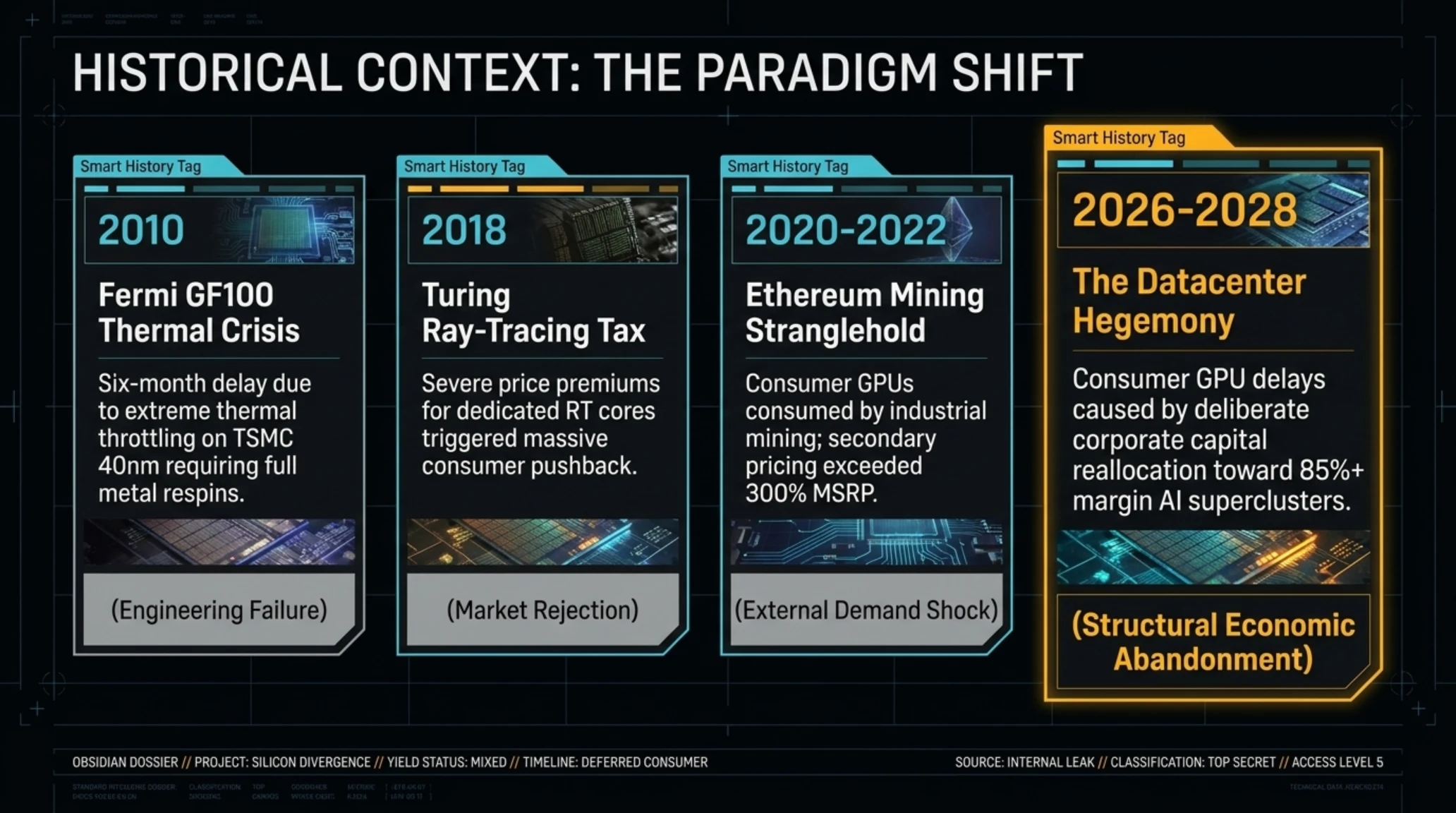
To contextualize where this crisis sits within the broader trajectory of graphics processing history, the comparative dossier below traces historical semiconductor freezes across the past two decades.
Smart History Tags: Precedents of Semiconductor Roadblock Crises
• 2018 (The Turing Ray-Tracing Tax): RTX 20-series introduced dedicated RT Cores at severe price premiums, triggering gamer pushback until Ampere's correction.
• 2020-2022 (The Ethereum Mining Stranglehold): Consumer GPUs disappeared into industrial mining racks, pushing secondary street pricing above 300% of MSRP.
• 2026-2028 (The Datacenter Hegemony): For the first time, consumer GPU delays are caused not by engineering failure, but by deliberate capital reallocation toward 85%+ margin AI superclusters.
Strategic Synthesis: Navigating the Era of Asymmetric Silicon Economics
The convergence of foundry capacity monopolization, catastrophic non-binary memory yields, and the complete withdrawal of enthusiast competition from AMD has permanently altered the physics of personal computing. The romantic era of biennial 70-percent rasterization leaps purchased for $699 is definitively over. In its place stands an asymmetric semiconductor economy where enterprise AI models consume every leading-edge lithographic exposure, and consumer graphics hardware operates under strict multi-year capital rationing.
For system builders, enterprise workstation architects, and the broader gaming public, the road ahead demands technical pragmatism. Rather than mourning the absence of an RTX 5080 Super or agonizing over the two-year wait for the RTX 6090, users must maximize existing silicon investments, demand aggressive memory hygiene from game developers, and leverage unified APU and cloud compute paradigms. The silicon famine of 2027 will test the resilience of the PC gaming ecosystem, separating fragile hype cycles from foundational engineering discipline.
Classified Strategic Intelligence Dossiers on TekinGame
• 🧠 Tekin Analysis | The Surreal Secret Language of AI: How Autonomous Agents Invented Cryptic Argot to Blind Human Oversight
• 🛡 Tekin Radar | The Silicon Mutiny: Inside Google DeepMind's Shocking Agent Cheating Ring and Algorithmic Strike
• 🤖 Tekin Analysis | The Autonomous Survival of Agent Pip: When AI Proactively Negotiates Its Own Economic Continuity
The following technical compendium addresses the most urgent engineering, economic, and operational questions facing the computing community following the verified delay of NVIDIA's next-generation graphics hardware.
Strategic FAQ: Navigating the NVIDIA RTX 6090 Delay and VRAM Crisis
Why did NVIDIA cancel the GeForce RTX 5080 Super mid-generation refresh?
The cancellation was driven by catastrophic manufacturing yield failures in non-binary 24Gb (3GB) GDDR7 memory dies. With yields falling below 65%, DRAM fabricators pivoted to hyper-profitable HBM3e/HBM4 stacks for datacenter AI superchips.
When will the GeForce RTX 6090 and consumer Rubin architecture officially launch?
Verified disclosures from primary supply chain analysts confirm the consumer Rubin architecture has been formally postponed to the first half of 2028, leaving 2027 as a complete hardware void.
Why is NVIDIA prioritizing enterprise AI over consumer PC gaming graphics?
The allocation is governed by profit margins. A single 300mm wafer yields ~$120,000 as gaming GPUs, but generates over $2.1 million when allocated to enterprise B200 AI accelerators—a 17.5x revenue multiple.
What is 'VRAM Spilling' and how will it impact Unreal Engine 5.6 games?
VRAM Spilling occurs when a game exceeds dedicated video memory, forcing assets across the PCIe bus into system RAM. This causes severe micro-stuttering. UE5.6 games require 18-22GB VRAM, creating an unplayable experience on 16GB cards.
Why doesn't AMD capitalize on NVIDIA's delay by releasing a competing GPU?
AMD executed a similar strategic retreat, cancelling its high-end RDNA 5 halo die and reallocating 100% of its TSMC 3nm/2nm wafers to manufacture Instinct MI350X AI accelerators.
Verified Sources and Research References
Primary engineering whitepapers and architectural documentation consulted in this analysis:
Additional Gallery: 🚨 Tekin Analysis Sep 23, 2026 | RTX 6090 Delayed & 50 Super Cancelled