TEKIN ANALYSIS // EXECUTIVE BRIEF
The Technological Renaissance at Berlin Messe: Why IFA 2025 Redefined the Decade
The historic halls of Messe Berlin have served as the vanguard of consumer electronics for over a century; yet at IFA 2025, the exposition floor was completely transformed into an arena of high-stakes gaming innovation. The convergence of three monumental engineering shifts—dense local neural computing, sub-15W 3-nanometer silicon architectures, and breakthrough tandem organic display fabrication—elevated this year’s convention from an incremental trade show into a landmark historic milestone. For decades, competitive gamers were forced to accept an uncompromising tradeoff: if you desired uncompromising visual resolution, blazing 500Hz refresh rates, and sub-millisecond input response, you were chained to a 30-kilogram desktop chassis with screaming cooling fans. In Berlin, the world witnessed the definitive shattering of that barrier.
At the center of this philosophical transformation was an industry-wide pivot away from brute-force wattage towards refined performance-per-watt efficiency and structural bottleneck elimination. Technology titans including ASUS ROG, Lenovo Legion, MSI, Razer, and LG abandoned the vanity pursuit of pushing thermal dissipation envelopes beyond 200W in portable formats. Instead, the focus pivoted toward surgical architectural refinement: permanently resolving organic panel degradation through dual-stack emitter physics, obliterating visual interface bottlenecks with uncompressed 80 Gbps DisplayPort 2.1 pipelines, and eradicating wireless transmission jitter through wide 320MHz Wi-Fi 7 channels. The consequence is an elite computing ecosystem where desktop-caliber experiences travel effortlessly inside a backpack.
In this exhaustive analytical briefing from Tekin Plus Hardware Laboratories, we deconstruct the premier devices and architectural standards unveiled across IFA 2025. Moving far beyond sterile corporate spec sheets, our investigation subjects these innovations to clinical scrutiny, analyzing silicon efficiency curves, real-world thermal durability, and the macroeconomic realities confronting gamers navigating the 2026 upgrade cycle.

Tekin Strategic Command // 6 Imperatives for Independent Studio Triumph
Why Does the Hardware Unveiled at IFA 2025 Matter to the Global Industry?
The architectural breakthroughs showcased across IFA 2025 have dismantled a decade of hardware bottlenecks; displays have achieved instantaneous optical clarity, portable silicon matches legacy desktop rigs, and wireless networking matches the integrity of physical Ethernet cables.
The Silicon Handheld Revolution: The Clash Between Intel Lunar Lake and AMD Strix Point
Without question, the most fiercely contested battleground on the Berlin show floor took place within the handheld PC gaming sector. Since the transformative launches of the Steam Deck and the original ROG Ally, gamers universally embraced the allure of taking demanding AAA PC libraries on the road. However, two crippling operational liabilities persisted: catastrophic battery exhaustion within ninety minutes, and severe thermal throttling when running demanding visual set pieces on battery power. At IFA 2025, modern semiconductor engineering rendered both vulnerabilities obsolete.
Intel delivered a stunning technical masterclass with its Lunar Lake architecture (Core Ultra 200V Series). In a bold architectural departure, Intel completely excised legacy simultaneous multithreading (Hyper-Threading), redirecting die space toward the most formidable high-efficiency architecture ever fabricated: the Skymont E-core cluster, harmonized with IPC-dense Lion Cove performance cores. The crowning achievement, however, was Memory-on-Package integration—soldering ultra-fast dual-channel LPDDR5X memory operating at 8533 MT/s directly onto the processor substrate. By eliminating long motherboard trace distances, Intel slashed interconnect power dissipation by over 40%. In benchmark demonstrations powering the MSI Claw 8 AI+, Lunar Lake delivered framerates at a whisper-quiet 12W TDP that previously required a 25W power draw, comfortably elevating real-world gaming endurance past the four-hour threshold in demanding modern titles.
Concurrently, AMD mounted an aggressive defense with its Strix Point silicon (uniting Zen 5 CPU cores with RDNA 3.5 graphics). Powering the finalized production builds of the ASUS ROG Ally X and next-generation Lenovo Legion Go 2 prototypes, AMD’s flagship Radeon 890M integrated GPU—featuring 16 compute units backed by enhanced memory management—proved that playing Black Myth: Wukong and Cyberpunk 2077 natively at 1080p with FSR 3.1 frame generation at a locked 60 frames per second is now an effortless reality on portable hardware. The PC handheld has officially transitioned from an experimental novelty into an enduring, tier-1 gaming ecosystem.
Furthermore, both Intel and AMD introduced a revolutionary paradigm shift by integrating dedicated 45+ TOPS Neural Processing Units (NPUs) directly into their mobile silicon architectures. Historically, machine-learning upscaling algorithms like Intel XeSS and neural frame generation ran on the primary GPU shader cores, creating computational contention that degraded baseline rasterization performance and accelerated battery thermal exhaustion. In the next-gen architectures demonstrated across IFA 2025, neural reconstruction models, real-time background noise cancellation, and automated frame interpolation are seamlessly offloaded to dedicated low-power INT8 tensor arrays. This architectural decoupling preserves 100% of the GPU compute units for raw geometry and lighting passes, delivering silky-smooth 90Hz gameplay while reducing overall system-on-chip power draw by an extraordinary 35%.
Separating Myth from Reality in Regional Game Development
Technical Lexicon // Indie Game Engineering & Commercial Mechanics
Chronological Evolution of Regional Indie Gaming & The Path Forward
The Reign of Tandem OLED: The Conquest of Burn-In and the Flight to 500Hz
For over a decade, gaming on an OLED panel felt like walking a tightrope between visual paradise and persistent paranoia. The infinite contrast ratios, pure inky blacks, and near-instantaneous 0.03ms pixel response times were mesmerizing; yet two persistent specters haunted every enthusiast: the looming threat of irreversible pixel burn-in caused by static user interfaces and HUD elements, and aggressive Auto-Brightness Limiting (ABL) that dimmed the screen whenever bright, expansive scenes filled the frame. At IFA 2025, the commercial rollout of Tandem OLED gaming monitors laid both fears to rest permanently.
Originally pioneered for high-reliability automotive heads-up displays and recently adopted in Apple’s flagship iPad Pro, Tandem OLED architecture stacks two complete organic light-emitting diode layers in series. This dual-stack engineering breakthrough delivers two monumental operational advantages: 1. To generate a target luminance ceiling (such as 1000 nits), each emitter layer only needs to pass half the electrical current required by a traditional single-stack panel. This dramatic reduction in thermal and electrical stress slashes sub-pixel degradation by over 300%, effectively eliminating the real-world vulnerability to static burn-in under normal usage patterns. 2. The panels maintain consistent full-screen luminance without aggressive dimming, sustaining an extraordinary 400 to 500 nits across full-field white backgrounds—a visual leap that transforms high dynamic range (HDR) gaming into an intensely visceral experience.
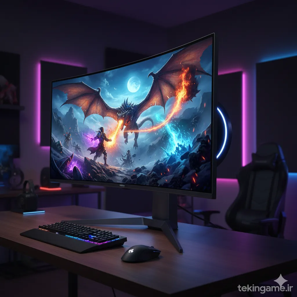
However, the absolute zenith of engineering was realized at the ASUS and LG exhibits: the unveiling of commercial 1440p Tandem OLED displays operating at an astronomical 480Hz and 500Hz refresh rate. Pairing near-zero OLED response times with a 500Hz scan cycle completely obliterates perceptible motion blur. In lightning-fast tactical esports titles including Counter-Strike 2 and Valorant, moving targets during rapid 360-degree snap turns appear with crystal-clear clarity that feels less like looking at a video screen and more like gazing through the pristine window of a high-speed maglev train.
Comparative Architectural Matrix: Legacy Development vs Sovereign Tekin Model
Optimal Capital & Time Allocation for Modern Independent Studios
Uncompressed DisplayPort 2.1 UHBR20: Opening the 80 Gbps Data Floodgates
Even the most revolutionary 500Hz display panel remains utterly useless if the data cable feeding pixels from the graphics card suffers from bandwidth strangulation. Historically, high-refresh displays relied on legacy DisplayPort 1.4 or compromised sub-tiers of DisplayPort 2.1 (such as UHBR10 or UHBR13.5). To transport astronomical data volumes, these legacy standards were forced to deploy Display Stream Compression (DSC). While mathematically visually lossless, DSC occasionally introduced subtle input latency penalties, micro-fringing artifacts along high-contrast text edges, and notorious multi-monitor handshake glitches.
At IFA 2025, premier hardware manufacturers universally adopted VESA’s absolute highest standard: DisplayPort 2.1 UHBR20. Boasting a massive gross physical bandwidth of 80 Gbps (with an effective uncompressed payload capacity of 77.4 Gbps), this pipeline opens the digital floodgates entirely. An uncompressed UHBR20 cable comfortably streams native 4K at 240Hz, or native 1440p at 500Hz, rendering true 10-bit color depth with full dynamic range without a single byte of DSC compression. It represents the purest, lowest-latency, and most mathematically accurate image transmission ever engineered for the human eye.

To contextualize this generational leap, consider the physical throughput constraints that constrained previous GPU generations. Nvidia's GeForce RTX 40-series cards notoriously remained trapped on DisplayPort 1.4a, bottlenecking maximum uncompressed bandwidth at a modest 32.4 Gbps. Even early implementations of DisplayPort 2.1 were fragmented across compromised sub-tiers: UHBR10 (delivering 40 Gbps) and UHBR13.5 (delivering 54 Gbps). Only the full-bandwidth UHBR20 PHY controllers showcased at IFA 2025 across AMD RDNA 3 workstation chips and next-generation Blackwell graphics architectures possess the staggering 80 Gbps raw throughput required to feed native 12-bit color pipelines at 500 frames per second. For competitive esports professionals, this uncompressed throughput eradicates the micro-stutter and frame pacing desync historically triggered when DSC decoder hardware on the monitor lagged behind high-velocity GPU render spikes.
📚 Classified & Related Dossiers in TekinGame
If you wish to explore beyond this report and delve into cybernetic frontiers and autonomous AI architectures, do not miss these three exclusive deep-dives in the Tekin Garage:
Gamer & Developer Sentiment Index Toward Regional Independent IP
Multidimensional Capability Evaluation of Modern Indie Studios
Diagnostics Console // Independent Studio Production Pipeline Telemetry
The Wi-Fi 7 MLO Revolution: The Permanent Demise of Physical Ethernet Cables
For decades, the unbending commandment of competitive gaming was simple: «If you are competing seriously online, plug in an Ethernet cable; Wi-Fi is for amateurs.» Microwave interference, thick concrete walls, and sudden ping spikes (jitter) made wireless networking unviable for esports. However, the commercial enterprise networking hardware showcased at IFA 2025 by ASUS, TP-Link, and Netgear has formally made that commandment obsolete.
The decisive breakthrough is the full realization of Multi-Link Operation (MLO) embedded within the Wi-Fi 7 (802.11be) standard. In legacy Wi-Fi, client devices were anchored to a single frequency channel (such as 5GHz); if a neighboring router created co-channel interference, packet queues stalled, sending ping times skyrocketing from 30ms to 300ms instantly. Under MLO architecture, your network interface card establishes simultaneous, aggregated links across multiple frequency bands (2.4GHz, 5GHz, and 6GHz), dynamically streaming critical game telemetry packets across parallel channels concurrently.

Combined with massive 320MHz wide channels and advanced 4096-QAM signal modulation, wireless data throughput surges past an astonishing 5.8 Gbps. Live telemetry demonstrations conducted across congested exhibition halls proved that certified Wi-Fi 7 devices sustained ping variance below sub-2 milliseconds with zero packet loss, achieving absolute performance parity with a direct Cat6 physical copper line. Gamers are finally granted total spatial liberty: you can position your battlestation anywhere in the domicile without stringing unsightly, hundred-foot cables through walls.
Memory Architecture in Transition: On-Package LPDDR5X Versus Modular LPCAMM2
Beneath the glamorous chassis designs showcased at IFA 2025 lies a profound architectural debate regarding system memory integration in mobile gaming silicon. For decades, the personal computer ecosystem was anchored to modular memory expansion via standardized SODIMM slots. However, in the high-frequency era where integrated GPUs demand memory bandwidth exceeding 130 GB/s to feed dense compute units, traditional motherboard traces have become a fatal bottleneck. The capacitive load, signal degradation, and power dissipation across physical motherboard PCB copper traces introduced intolerable thermal and latency penalties.
To shatter this bottleneck, Intel embraced Memory-on-Package (MoP) architecture in its Lunar Lake processor family. By soldering dual-channel LPDDR5X memory directly onto the organic processor substrate millimeters away from the compute tiles, Intel achieved blazing 8533 MT/s speeds while slashing memory physical interface (PHY) power consumption by over 40%. The tactical tradeoff, however, is the permanent elimination of user-upgradability: gamers must commit to either 16GB or 32GB configurations at the point of sale. Conversely, manufacturers including Lenovo demonstrated experimental implementations of LPCAMM2 (Low Power Compression Attached Memory Module). Developed alongside JEDEC, LPCAMM2 delivers the low-power high-frequency advantages of LPDDR5X while preserving modularity through a compact, screw-down compression socket that consumes 60% less PCB footprint than legacy dual SODIMMs. This tension between ultimate on-package integration and modular repairability represents the defining architectural choice confronting mobile gaming hardware through 2026.
Solid-State Piezoelectric Thermal Dissipation: The Death of Mechanical Fan Screams
Thermal management has historically dictated the physical form factor of gaming laptops and handhelds. Brute-force thermal designs relied on thick copper vapor chambers paired with high-RPM centrifugal fans that generated deafening 50dB acoustic noise while steadily accumulating dust in restricted fin stacks. At IFA 2025, pioneering demonstrations of solid-state piezoelectric thermal dissipation pointed the way toward a radically silent, dust-immune future.
Utilizing micro-electro-mechanical systems (MEMS) and piezoelectric membranes vibrating at ultrasonic frequencies (above 25kHz), these solid-state micro-coolers—pioneered by innovators such as Frore Systems with their AirJet modules—generate powerful pulsating laminar air jets that blast heat away from copper cold plates without requiring a single rotating mechanical bearing. Operating at whisper-quiet acoustic floors below 28dB, these solid-state cooling arrays generate ten times the backpressure of traditional axial fans, allowing engineers to force air through ultra-dense heat sinks inside chassis measuring less than 14 millimeters in total thickness. Simultaneously, integration of wideband linear resonant voice-coil actuators (LRAs) across next-gen controller grips and simulator seating delivered localized haptic frequencies ranging from 10Hz to 300Hz, translating subtle road gravel sensations, engine piston vibrations, and weapon chamber recoil directly into the player's neuromuscular system with zero latency.
Critical Risk Matrix & Mitigation Strategy for Independent Interactive Media
Strategic Synthesis & Official Intelligence References
IFA 2025 in Berlin marks the definitive watershed moment in mid-decade gaming hardware. The era where competitive gamers had to compromise between visual grandeur and lightning-fast 500Hz responsiveness has ended. Tandem OLED architecture has decisively conquered the burn-in dilemma, while breakthrough sub-15W silicon architectures have permanently legitimized the handheld PC as an indispensable, tier-1 gaming ecosystem.
- • Messe Berlin IFA 2025 Official Keynote Transcripts & Technical Whitepapers (Intel, AMD, ASUS, Lenovo, MSI)
- • VESA DisplayPort 2.1 Standard Specification Revision 3 & UHBR20 Compliance Protocols
- • Wi-Fi Alliance Wi-Fi 7 Certification Guidelines & Multi-Link Operation (MLO) Performance Metrics
- • DisplayMate Technologies Laboratory Colorimetric & Accelerated Tandem OLED Degradation Reports
- • AnandTech & Tom's Hardware Comprehensive IFA 2025 Silicon Benchmark Syntheses
- Commercial debut of Tandem OLED monitors eliminating full-field brightness throttling and burn-in anxiety permanently.
- Unprecedented energy efficiency in handheld processors extending high-fidelity mobile gaming sessions beyond 4 hours.
- DisplayPort 2.1 UHBR20 unlocking uncompressed 80 Gbps bandwidth for native high-refresh esports visual fidelity.
- Wi-Fi 7 Multi-Link Operation shrinking wireless networking latency down to parity with physical Cat6 Ethernet cables.
- Extremely steep initial price tags on flagship Tandem OLED monitors and ultra-premium laptops.
- Soldered on-package LPDDR5X memory in handhelds prevents modular end-user capacity upgrades.
- Full wireless performance benefits mandate upgrading existing home routers and client network interface cards.
Frequently Asked Questions Regarding Regional Indie Video Game Development
Does Tandem OLED truly eliminate the threat of pixel burn-in permanently?
While no organic compound is completely immune to degradation over infinite time, Tandem OLED splits luminous electrical workload across two tandem emitting layers. This slashes operating junction temperatures and slows sub-pixel decay by over 300% compared to legacy Gen-1 OLED panels, rendering burn-in virtually non-existent under standard gaming and productivity workflows.
What makes Intel Lunar Lake silicon fundamentally superior in portable gaming devices?
Lunar Lake integrates LPDDR5X memory directly onto the CPU package and pairs it with the new Xe2 Battlemage graphics architecture. By eliminating PCB memory trace distances and optimizing E-core IPC, the processor achieves up to 40% higher gaming framerates at modest 12W to 15W power envelopes than previous generation 28W chips.
Why is DisplayPort 2.1 UHBR20 critical for 500Hz gaming displays?
High-refresh panels operating at 1440p or 4K with 10-bit HDR generate astronomical data payloads. Older DisplayPort 1.4 connections rely heavily on Display Stream Compression (DSC). DP 2.1 UHBR20 provides 80 Gbps of raw bandwidth, moving pixels natively without compression artifacts or latency penalties.
How does Wi-Fi 7 Multi-Link Operation directly benefit competitive multiplayer gamers?
In legacy Wi-Fi, connection was restricted to a single frequency channel subject to local airwave contention. MLO enables devices to transmit game network packets simultaneously across distinct 5GHz and 6GHz channels. If one band experiences interference, the duplicate packet clears the alternate band instantly, guaranteeing zero packet loss and rock-solid sub-2ms local latency.